Potting PCB: A Comprehensive Guide to Protecting Printed Circuit Boards
Introduction
Printed Circuit Boards (PCBs) are the backbone of modern electronics, found in everything from consumer gadgets to industrial machinery. However, PCBs are often exposed to harsh environments, including moisture, dust, chemicals, and mechanical stress, which can lead to failure. Potting is a widely used technique to protect PCBs by encapsulating them in a protective material.
This article explores the process of potting PCBs, the materials used, benefits, challenges, and best practices for effective potting.
1. What is PCB Potting?
Potting involves filling an electronic assembly (such as a PCB) with a liquid compound that hardens into a solid protective layer. This process shields the PCB from:
- Moisture and corrosion
- Dust and contaminants
- Vibration and mechanical shock
- Chemical exposure
- Thermal stress
Potting is commonly used in automotive, aerospace, marine, and industrial electronics, where reliability is critical.
2. Potting Materials
The choice of potting material depends on the application requirements. The most common types are:
A. Epoxy Resins
- Pros: High mechanical strength, excellent chemical resistance, good adhesion.
- Cons: Can be brittle, may generate heat during curing.
- Applications: Industrial controls, power electronics.
B. Polyurethane (PU)
- Pros: Flexible, good moisture resistance, absorbs vibrations.
- Cons: Lower thermal resistance than epoxy.
- Applications: Automotive sensors, outdoor electronics.
C. Silicone
- Pros: Extreme temperature resistance (-50°C to 200°C), flexible, UV resistant.
- Cons: Expensive, lower mechanical strength.
- Applications: High-temperature environments, LED lighting.
D. Acrylics
- Pros: Fast curing, reworkable, good electrical insulation.
- Cons: Lower chemical resistance.
- Applications: Consumer electronics, prototypes.
3. The Potting Process
Step 1: PCB Preparation
- Clean the PCB to remove dust, flux residues, and moisture.
- Apply conformal coating (if needed) for additional protection.
Step 2: Selecting the Potting Compound
- Choose based on thermal, mechanical, and environmental requirements.
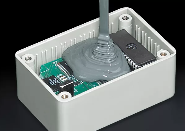
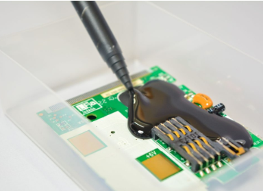
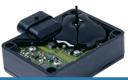
Step 3: Encapsulation
- Place the PCB in a mold or enclosure.
- Pour or inject the potting compound carefully to avoid air bubbles.
Step 4: Curing
- Allow the material to cure at room temperature or with heat acceleration.
Step 5: Inspection & Testing
- Check for voids, cracks, or incomplete coverage.
- Perform electrical and environmental testing.
4. Benefits of Potting PCBs
✅ Enhanced Durability – Protects against physical damage.
✅ Improved Thermal Management – Some compounds dissipate heat effectively.
✅ Electrical Insulation – Prevents short circuits.
✅ Chemical & Moisture Resistance – Ideal for harsh environments.
✅ Vibration Damping – Critical for automotive and aerospace applications.
5. Challenges & Considerations
A. Air Entrapment
- Bubbles can weaken protection. Vacuum potting helps eliminate trapped air.
B. Thermal Expansion Mismatch
- Different coefficients of expansion can stress components.
C. Rework Difficulty
- Once potted, repairs become challenging (except with acrylics).
D. Cost
- High-performance materials (e.g., silicone) can be expensive.
6. Best Practices for Effective Potting
✔ Use Degassing for Bubble-Free Potting
✔ Select the Right Material for the Environment
✔ Ensure Proper Mixing of Two-Part Compounds
✔ Control Curing Conditions (Temperature & Humidity)
✔ Test Small Batches Before Full Production
7. Applications of Potting in Electronics
- Automotive: ECU modules, sensors.
- Aerospace: Avionics, satellite electronics.
- Marine: Navigation systems, underwater devices.
- Industrial: Motor controllers, power supplies.
- Renewable Energy: Solar inverters, wind turbine controls.
Conclusion
Potting PCBs is a critical process for ensuring long-term reliability in demanding environments. By selecting the right material, following best practices, and addressing potential challenges, manufacturers can enhance the durability and performance of electronic assemblies.
As technology advances, new potting materials and techniques (such as 3D-printed encapsulation) are emerging, offering even better protection for next-generation electronics.