Fusible PCBs: Design, Applications, and Future Trends
1. Introduction
Printed Circuit Boards (PCBs) are essential components in modern electronics, providing mechanical support and electrical connections for electronic components. Among the various types of PCBs, fusible PCBs represent a specialized category designed to enhance safety and reliability in electrical circuits. These PCBs incorporate fusible links or fusible traces that act as sacrificial elements, breaking the circuit under excessive current conditions to prevent damage to sensitive components.
This article explores the design principles, materials, manufacturing processes, applications, and future trends of fusible PCBs.
2. What Are Fusible PCBs?
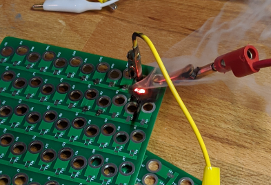
Fusible PCBs are printed circuit boards that integrate fusible elements—thin conductive traces or embedded fuses—that melt or break when subjected to overcurrent conditions. These elements function similarly to traditional fuses but are integrated directly into the PCB layout, eliminating the need for discrete fuse components.
Key Characteristics:
- Controlled Trace Width: Fusible traces are designed with precise widths to ensure they melt at a predetermined current.
- Material Selection: High-resistance or low-melting-point materials (e.g., thin copper, tin alloys) are used.
- Self-Resetting or One-Time Use: Some fusible PCBs use resettable fuses (PTCs), while others rely on one-time sacrificial traces.

3. Design Considerations for Fusible PCBs
Designing a fusible PCB requires careful consideration of electrical, thermal, and mechanical factors.
3.1 Trace Geometry and Current Rating
- Narrow Traces: Fusible traces are intentionally narrower than standard traces to increase resistance and heat generation.
- Current vs. Trace Width: The relationship follows IPC-2221 standards, where trace width determines current-carrying capacity.
- Thermal Management: Adjacent components must be protected from heat generated during fuse activation.
3.2 Material Selection
- Copper Thickness: Thinner copper (e.g., 0.5 oz/ft²) melts more easily than thicker layers.
- Alternative Fusible Materials: Some designs use tin-lead alloys or conductive polymers for precise fusing behavior.
3.3 Placement and Isolation
- Strategic Location: Fusible traces should be placed near power inputs or sensitive components.
- Isolation Gaps: To prevent arcing after fusing, isolation gaps or slots may be incorporated.
3.4 Simulation and Testing
- Finite Element Analysis (FEA): Simulates thermal and electrical behavior under fault conditions.
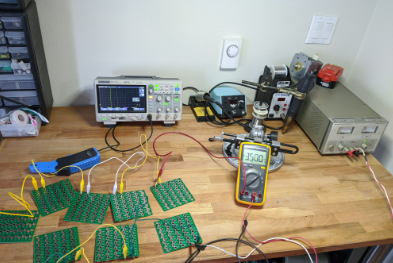
- Prototype Testing: Real-world testing ensures the fusible element operates as intended.
4. Manufacturing Processes
Fusible PCBs follow standard PCB fabrication techniques with additional considerations:
4.1 Etching and Trace Formation
- Precision Etching: Laser or chemical etching ensures accurate trace widths.
- Selective Plating: Some fusible traces may use different plating materials.
4.2 Embedding Fusible Elements
- Discrete Fuse Integration: Some PCBs embed chip fuses or PTC resettable fuses within layers.
- Laser-Drilled Fusible Links: Used in high-density designs where space is limited.
4.3 Quality Control
- Current Testing: Each fusible PCB must be tested to verify fusing behavior.
- Environmental Stress Testing: Ensures reliability under varying temperatures and humidity levels.
5. Applications of Fusible PCBs
Fusible PCBs are used in industries where overcurrent protection is critical:
5.1 Consumer Electronics
- Smartphones & Laptops: Protect charging circuits from short circuits.
- Power Supplies: Prevent damage from voltage surges.
5.2 Automotive Electronics
- EV Battery Management Systems (BMS): Fusible traces prevent thermal runaway.
- Infotainment Systems: Protect against electrical faults.
5.3 Industrial and Power Electronics
- Motor Drives: Prevent damage from overloads.
- Renewable Energy Systems: Solar inverters use fusible PCBs for surge protection.
5.4 Medical Devices
- Implantable Electronics: Fail-safe mechanisms ensure patient safety.
- Diagnostic Equipment: Prevents damage from electrical faults.

6. Advantages and Limitations
6.1 Advantages
✔ Space-Saving: Eliminates the need for external fuses.
✔ Cost-Effective: Reduces component count.
✔ Customizable: Fusing behavior can be tailored to specific needs.
6.2 Limitations
✖ One-Time Use (Non-Resettable): Some designs require PCB replacement after fusing.
✖ Precision Required: Poor design can lead to unintended fuse activation or failure.
7. Future Trends in Fusible PCBs
The evolution of fusible PCBs is driven by advancements in materials and manufacturing:
7.1 Self-Healing Materials
- Conductive Polymers: Research is ongoing into materials that can self-repair after fusing.
7.2 Additive Manufacturing (3D Printing)
- Printed Fusible Traces: Enables rapid prototyping of custom fusible PCBs.
7.3 AI-Optimized Designs
- Machine Learning Algorithms: Can predict optimal trace geometries for specific applications.
7.4 Integration with IoT
- Smart Fusing: PCBs with embedded sensors that report fuse status remotely.
8. Conclusion
Fusible PCBs offer a compact, reliable, and cost-effective solution for overcurrent protection in modern electronics. By integrating sacrificial traces or embedded fuses, these PCBs enhance safety without requiring additional components. Future advancements in materials science, additive manufacturing, and AI-driven design will further expand their applications.
As electronics continue to evolve, fusible PCBs will play an increasingly important role in ensuring device reliability and user safety.


