PCB and SMT Integration Techniques for Streamlined Manufacturing
Key Takeaways
Effective integration of PCB assembly and SMT processes hinges on optimizing workflows to eliminate redundancies while maintaining precision. By aligning design for manufacturability (DFM) principles with SMT placement strategies, manufacturers reduce errors and accelerate production cycles. A critical focus lies in leveraging PCBA (printed circuit board assembly) advancements, such as automated optical inspection (AOI), to ensure component accuracy and solder joint integrity.
Cost efficiency emerges from harmonizing PCB layout with SMT capabilities—for instance, minimizing panel waste through intelligent footprint planning. Additionally, adopting unified design-software platforms bridges gaps between PCB design and SMT assembly teams, enabling real-time collaboration. This synergy not only slashes prototyping costs but also enhances scalability for high-volume production.
Reliability gains are achieved by integrating thermal management features early in PCB design, which prevents solder reflow issues during SMT processes. Advanced techniques like 3D solder paste inspection (SPI) further mitigate defects, ensuring consistent PCBA quality. Ultimately, streamlined workflows and cross-disciplinary alignment position manufacturers to meet evolving demands for compact, high-performance electronics.
PCB/SMT Workflow Optimization Techniques
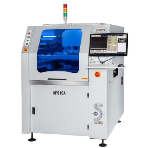
Optimizing PCB assembly workflows requires strategic alignment between design, fabrication, and SMT processes. A critical first step involves adopting design for manufacturability (DFM) principles to minimize rework during PCBA stages. By integrating automated optical inspection (AOI) systems early in the SMT line, manufacturers can detect solder paste defects or component misalignments in real time, reducing post-assembly corrections.
| Workflow Stage | Traditional Approach | Optimized Approach |
|---|---|---|
| Design Validation | Manual DFM checks | AI-driven DFM analysis |
| Component Placement | Sequential programming | Parallelized setups |
| Quality Assurance | Post-assembly testing | In-line AOI integration |
Leveraging modular tooling in SMT lines further enhances flexibility, allowing rapid transitions between high-mix, low-volume PCB assembly batches. For instance, synchronized stencil printers and pick-and-place machines can reduce idle time by 30–40%, directly improving throughput. Additionally, implementing closed-loop feedback between PCBA testing and design teams ensures iterative improvements, such as optimizing pad geometries for better solder joint reliability. These techniques not only streamline workflows but also create a foundation for scalable, cost-efficient manufacturing ecosystems.
Cost-Effective PCB and SMT Integration
Achieving cost efficiency in PCB assembly requires strategic alignment between design, materials, and SMT processes. By optimizing design-for-manufacturability (DFM) principles, engineers can minimize material waste and reduce rework during PCBA production. For instance, standardizing component footprints and panelization layouts lowers setup times and enhances throughput in high-volume SMT lines.
Tip: Prioritize component sourcing from suppliers offering bulk pricing for high-usage parts to reduce BOM costs without compromising quality.
Integrating automated optical inspection (AOI) systems with SMT assembly workflows ensures early defect detection, preventing costly post-production corrections. Additionally, leveraging mixed-technology boards—combining surface-mount and through-hole components—can balance performance requirements with budget constraints. Thermal management optimizations, such as selecting cost-effective solder pastes with optimal reflow profiles, further enhance yield rates.
A critical factor in cost-effective integration is the synergy between PCB layout and SMT equipment capabilities. Designing boards with uniform pad sizes and spacing minimizes nozzle changes in pick-and-place machines, accelerating assembly cycles. Collaborative partnerships with PCBA service providers offering scalable pricing models (e.g., tiered volumes or shared tooling costs) also contribute to long-term savings.
"Adopting modular design frameworks allows reuse of validated circuit blocks across projects, slashing development costs by up to 30%."
By aligning design choices with manufacturing realities, businesses achieve a holistic cost structure that maintains reliability while meeting aggressive budget targets.
Advanced SMT Assembly for PCB Reliability
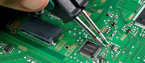
Modern PCB assembly processes leverage surface-mount technology (SMT) to achieve unprecedented levels of reliability in electronic manufacturing. By integrating precision placement systems and automated optical inspection (AOI), manufacturers ensure that PCBA components adhere to exacting tolerances, minimizing defects such as solder bridging or tombstoning. Advanced reflow soldering profiles, optimized for specific PCB substrate materials, further enhance thermal management, reducing stress on delicate components during temperature cycling.
The adoption of high-speed pick-and-place machines paired with intelligent solder paste dispensing systems allows for consistent SMT assembly accuracy, even in high-density designs. This precision is critical for applications requiring PCB reliability, such as aerospace or medical devices, where component failure risks must be eliminated. Additionally, real-time monitoring during PCBA production enables rapid identification of process deviations, ensuring compliance with IPC-A-610 standards.
By aligning PCB assembly workflows with advanced SMT capabilities, manufacturers achieve tighter control over production variables, from component alignment to solder joint integrity. This synergy not only boosts product longevity but also supports seamless scalability in high-volume manufacturing environments.
Streamlined PCB Design Enhances SMT Efficiency
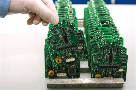
Modern PCB assembly processes demand precision-aligned designs to maximize SMT (Surface Mount Technology) efficiency. A streamlined PCB layout minimizes placement errors and solder bridging by optimizing pad geometries, solder mask apertures, and component spacing. For instance, reducing footprint mismatches between ICs and passive components ensures smoother PCBA workflows, as automated pick-and-place machines operate with higher accuracy.
Integrating design for manufacturability (DFM) principles directly into PCB schematics accelerates SMT assembly cycles. Techniques like standardized land patterns and symmetrical thermal reliefs prevent uneven heating during reflow soldering, a common cause of defects. Additionally, adopting unified layer stackup configurations enhances signal integrity while simplifying SMT feeder setups.
Advanced tools such as auto-router algorithms and 3D collision detection further refine design-to-production handoffs. By aligning PCB layout parameters with PCBA machine tolerances, manufacturers achieve first-pass yield improvements of up to 30%. This synergy not only reduces rework costs but also strengthens reliability in high-density applications like IoT modules or automotive electronics.
Ultimately, a harmonized approach to PCB design and SMT execution bridges the gap between prototyping and mass production, ensuring scalable, cost-efficient manufacturing outcomes.

Synergy in PCB Layout and SMT Assembly
Achieving seamless integration between PCB assembly processes and surface-mount technology (SMT) begins with strategic design alignment. Effective PCB layout directly influences SMT efficiency, as component placement, pad geometry, and trace routing dictate solder joint quality and automated placement accuracy. For instance, optimizing thermal relief patterns and copper balancing minimizes warpage during reflow soldering, enhancing reliability in PCBA outcomes.
Design-for-manufacturing (DFM) principles bridge this synergy, ensuring layouts accommodate SMT assembly constraints like pick-and-place machine tolerances and solder paste application precision. By embedding testability features (e.g., fiducial markers or test points) early in the design phase, manufacturers reduce post-assembly rework. Advanced tools like 3D modeling and thermal simulation further align layout decisions with SMT requirements, preventing hotspots or signal interference.
Transitioning from design to production, collaborative workflows between PCB designers and SMT engineers enable real-time adjustments. For example, adjusting component spacing to match stencil apertures improves solder paste deposition consistency. This interdependence ensures PCBA units meet both performance benchmarks and cost targets, solidifying the foundation for scalable, high-yield manufacturing.
Key Benefits of PCB/SMT Integration
Integrating PCB assembly and SMT processes unlocks significant advantages for modern electronics manufacturing. By harmonizing design and production workflows, manufacturers achieve faster turnaround times while maintaining stringent quality standards. The seamless coordination between PCBA stages reduces manual handling, minimizing errors and material waste. For instance, optimized solder paste application in SMT lines ensures precise component placement, directly enhancing PCB reliability in high-stress environments.
Another critical benefit lies in cost-efficiency. Unified PCB/SMT integration eliminates redundant steps, such as separate testing phases, by embedding quality checks within automated workflows. This approach not only accelerates production but also lowers per-unit costs—a key advantage for high-volume orders. Additionally, advanced thermal management techniques in integrated systems prevent warping during reflow soldering, ensuring consistent performance across PCBA batches.
The synergy between PCB layout and SMT assembly further improves scalability. Designers can leverage simulation tools to predict manufacturing outcomes, reducing trial runs and accelerating time-to-market. By aligning material selection with SMT capabilities—such as fine-pitch component compatibility—manufacturers achieve higher yield rates while maintaining flexibility for design iterations. These collaborative workflows position businesses to adapt swiftly to evolving technological demands without compromising on precision or durability.
Innovative Methods for PCB-SMT Manufacturing
Modern advancements in PCB assembly processes are reshaping how manufacturers integrate surface-mount technology (SMT) into production workflows. One groundbreaking approach involves combining additive manufacturing techniques with high-precision SMT placement systems, enabling rapid prototyping of complex PCBA designs. By leveraging laser-assisted solder paste deposition, manufacturers achieve micron-level accuracy while reducing material waste by up to 30%.
Another emerging method utilizes AI-driven optical inspection paired with real-time thermal profiling to optimize reflow soldering parameters. This integration minimizes defects in PCB assembly by dynamically adjusting heating zones based on component density and board geometry. For high-mix production environments, modular SMT pick-and-place systems with adaptive feeders are proving critical, cutting changeover times by 45% compared to traditional setups.
Innovators are also adopting hybrid PCBA strategies that merge rigid-flex PCB designs with embedded passive SMT components. This technique not only saves board space but enhances signal integrity in high-frequency applications. To further streamline workflows, manufacturers are implementing digital twin simulations that predict thermal stress points during SMT assembly, allowing preemptive design adjustments before physical production begins. These methods collectively address the dual challenges of scalability and precision in modern electronics manufacturing.
Conclusion
The convergence of PCB assembly and SMT technologies represents a transformative approach to modern electronics manufacturing. By harmonizing design-for-manufacturability principles with advanced PCBA workflows, manufacturers achieve unprecedented levels of precision and repeatability. This synergy reduces material waste, minimizes rework cycles, and accelerates time-to-market—critical factors in competitive industries.
Optimized PCB assembly processes, when paired with intelligent SMT placement strategies, create a robust framework for high-density interconnect (HDI) designs. The integration of real-time process monitoring and automated optical inspection (AOI) further ensures consistent quality across production batches. For PCBA projects, leveraging these methodologies translates to enhanced thermal management and mechanical stability, particularly in applications demanding miniaturization or extreme environmental resilience.
As manufacturers adopt these integrated systems, the focus shifts toward scalable solutions that balance cost-efficiency with technical sophistication. The result is a manufacturing ecosystem where SMT precision and PCB reliability coexist seamlessly, driving innovation while maintaining stringent compliance standards. Ultimately, this alignment positions businesses to meet evolving market demands without compromising on performance or profitability.
Frequently Asked Questions
How does integrated PCB assembly improve manufacturing efficiency?
Combining PCB assembly with SMT processes reduces manual intervention by automating component placement and soldering. This integration minimizes alignment errors and accelerates production cycles, particularly in high-volume PCBA projects.
What design factors are critical for SMT compatibility?
Thermal management and pad geometry directly affect SMT success. Designs must account for component spacing, solder mask alignment, and surface finish to prevent tombstoning or bridging during reflow.
Can existing PCB layouts be adapted for advanced SMT workflows?
Yes, but design-for-manufacturing (DFM) analysis is essential. Engineers often optimize trace routing, layer stacking, and fiducial marker placement to align with SMT pick-and-place machine requirements.
How does integrated PCB/SMT manufacturing reduce costs?
Unified PCB assembly workflows eliminate redundant quality checks and material waste. Bulk sourcing of substrates and SMT consumables further lowers per-unit costs in PCBA production.
What quality risks arise from poor PCB-SMT synergy?
Mismatched thermal profiles or inadequate solder paste volume can cause latent defects like cold joints. Rigorous in-circuit testing (ICT) and automated optical inspection (AOI) mitigate these risks in PCBA lines.
Optimize Your PCB Assembly Process Today
For tailored solutions in PCB assembly and SMT integration, please click here to explore advanced manufacturing options. Our expertise ensures seamless transitions from design to high-reliability PCBA production.