Surface Mount Technology (SMT) in PCB Manufacturing: A Comprehensive Overview
Introduction to Surface Mount Technology
Surface Mount Technology (SMT) has revolutionized the electronics manufacturing industry since its widespread adoption in the 1980s. As a method for producing electronic circuits, SMT involves mounting electronic components directly onto the surface of printed circuit boards (PCBs) rather than using the through-hole technology (THT) that dominated earlier decades. This technological shift has enabled the production of smaller, faster, and more reliable electronic devices that power our modern world.
The fundamental difference between SMT and traditional through-hole technology lies in the component mounting approach. While through-hole components require leads to be inserted into drilled holes and soldered on the opposite side, SMT components sit directly on the PCB surface, connecting via solder pads. This elimination of drilling requirements and lead insertion has transformed PCB design and manufacturing processes.
Historical Development of SMT
The origins of SMT can be traced back to the 1960s when IBM developed the Solid Logic Technology for their aerospace applications. However, it wasn’t until the 1980s that SMT gained widespread commercial acceptance. Several factors contributed to this adoption:
- Miniaturization demands: The consumer electronics boom required smaller components and higher circuit densities.
- Performance requirements: Higher frequency applications demanded reduced lead inductance.
- Manufacturing efficiency: SMT enabled greater automation and reduced production costs at scale.
- Reliability improvements: Surface-mounted joints proved more reliable in vibration-prone environments.
By the 1990s, SMT had become the dominant PCB assembly technology, with through-hole reserved for specific applications requiring mechanical strength or high power handling.
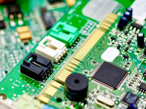
SMT Components and Their Characteristics
Surface mount devices (SMDs) come in standardized packages that differ significantly from their through-hole counterparts. These components are designed for machine placement and reflow soldering processes. The major categories include:
Passive Components
- Resistors and capacitors: Typically available in rectangular chip form (e.g., 0201, 0402, 0603, 0805, 1206 sizes)
- Inductors: Various package styles including chip and molded types
Active Components
- Small Outline Transistors (SOT): For diodes and transistors
- Small Outline Integrated Circuits (SOIC): Reduced versions of DIP packages
- Quad Flat Packages (QFP): For high pin count ICs with leads on all four sides
- Ball Grid Arrays (BGA): Using an array of solder balls for connection
- Chip Scale Packages (CSP): Nearly the size of the die itself
Specialized Components
- Microelectromechanical systems (MEMS): Sensors and actuators
- LED packages: Various surface mount LED configurations
Component packaging has continued to evolve, with trends toward smaller sizes (01005, 008004) and advanced packages like wafer-level chip-scale packages (WLCSP).
SMT PCB Design Considerations
Designing PCBs for surface mount technology requires attention to several critical factors:
Pad Design
Proper pad geometry is essential for reliable solder joints. Design considerations include:
- Pad size and shape relative to component terminations
- Thermal relief patterns for components requiring heat dissipation
- Solder mask definitions to prevent bridging
Component Placement
- Orientation consistency for automated assembly
- Minimum spacing requirements for pick-and-place machines
- Thermal management considerations for heat-generating components
Routing Considerations
- Trace width calculations based on current requirements
- Impedance control for high-speed signals
- Via placement strategies for dense designs
DFM (Design for Manufacturing) Principles
- Panelization considerations for efficient assembly
- Fiducial markers for machine vision alignment
- Test point accessibility for quality control
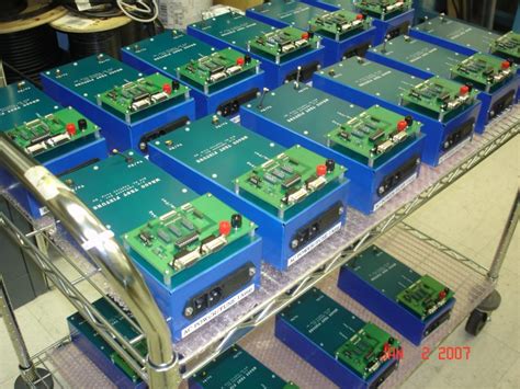
SMT Assembly Process
The SMT assembly process involves multiple precise steps:
- Solder Paste Application:
- Stencil printing is the most common method
- Laser-cut or electroformed stencils control paste deposition
- Solder paste composition (flux, alloy, particle size) is critical
- Component Placement:
- High-speed pick-and-place machines position components
- Vision systems ensure accurate alignment
- Placement speed can exceed 50,000 components per hour
- Reflow Soldering:
- The PCB passes through a multi-zone reflow oven
- Precise temperature profile management is crucial
- Typical profile stages: preheat, soak, reflow, cooling
- Inspection and Testing:
- Automated Optical Inspection (AOI) checks placement and solder quality
- X-ray inspection for hidden joints (e.g., BGA)
- Functional testing verifies circuit operation
- Secondary Operations (if needed):
- Through-hole component insertion and wave soldering
- Conformal coating application
- Final assembly and packaging
Advantages of SMT
The widespread adoption of SMT stems from its numerous advantages:
- Miniaturization:
- Smaller components enable more compact designs
- Components can be placed on both sides of the PCB
- Higher component density per unit area
- Performance Benefits:
- Reduced parasitic inductance and capacitance
- Better high-frequency performance
- Improved signal integrity in high-speed designs
- Manufacturing Efficiency:
- Higher automation levels reduce labor costs
- Faster assembly processes increase throughput
- Reduced drilling requirements lower production costs
- Reliability Improvements:
- Better mechanical performance under vibration
- More consistent solder joint formation
- Reduced susceptibility to thermal cycling damage
- Cost Effectiveness at Volume:
- Lower material costs for components
- Reduced board size requirements
- Economies of scale in high-volume production
Challenges and Limitations of SMT
Despite its advantages, SMT presents several challenges:
- Thermal Management Issues:
- Smaller components have less thermal mass
- Dense layouts can create hot spots
- Thermal expansion mismatches can cause stress
- Rework Difficulties:
- Small component sizes make manual rework challenging
- BGAs and other advanced packages require specialized equipment
- Multiple rework cycles can damage PCBs
- Mechanical Stress Vulnerabilities:
- Solder joints bear all mechanical loads
- Board flexure can crack joints
- Impact resistance may be reduced compared to through-hole
- Inspection Challenges:
- Hidden joints (like BGA) require X-ray inspection
- Small feature sizes challenge optical systems
- 3D inspection needed for proper solder joint evaluation
- Design Complexity:
- High-density designs require careful planning
- Signal integrity considerations become critical
- Thermal analysis is more demanding
Recent Advances in SMT
SMT continues to evolve with several notable advancements:
- Miniaturization Trends:
- 01005 (0.4mm × 0.2mm) and smaller components
- Ultra-fine pitch components (<0.3mm pitch)
- Embedded component technology
- Advanced Materials:
- Low-temperature solder alloys
- High-performance substrate materials
- Novel solder mask formulations
- Process Innovations:
- 3D solder paste printing
- Laser-assisted rework systems
- Advanced flux chemistries
- Inspection Technologies:
- AI-powered optical inspection
- High-resolution 3D AOI systems
- Real-time process monitoring
- Packaging Developments:
- Fan-out wafer-level packaging (FOWLP)
- System-in-Package (SiP) integration
- Heterogeneous integration techniques
Future Trends in SMT
The future of SMT points toward several key directions:
- Continued Miniaturization:
- Adoption of 008004 components (0.25mm × 0.125mm)
- Further reduction in component pitches
- Increased use of chip-scale packaging
- Advanced Assembly Techniques:
- Hybrid SMT/wafer-level assembly processes
- Multi-die integration approaches
- Adaptive placement systems for flexible electronics
- Materials Innovation:
- Sustainable solder alloys and fluxes
- High-reliability underfill materials
- Thermally conductive adhesives
- Smart Manufacturing Integration:
- IoT-enabled process monitoring
- Machine learning for process optimization
- Digital twin applications in SMT lines
- Specialized Applications:
- High-power SMT solutions
- Extreme environment electronics
- Biomedical implantable devices
Conclusion
Surface Mount Technology has become the backbone of modern electronics manufacturing, enabling the compact, high-performance devices we rely on daily. From smartphones to medical equipment, SMT’s contributions to miniaturization, reliability, and manufacturing efficiency cannot be overstated. As the technology continues to evolve, it faces challenges from ever-smaller component sizes, increasing performance demands, and the need for sustainable manufacturing practices. However, with ongoing advancements in materials, processes, and inspection technologies, SMT is well-positioned to meet these challenges and remain the dominant PCB assembly methodology for the foreseeable future. The continued innovation in SMT will play a crucial role in enabling next-generation electronic products across all industries.