PCB Edge Plating: A Comprehensive Guide to Design, Manufacturing, and Applications
Introduction to PCB Edge Plating
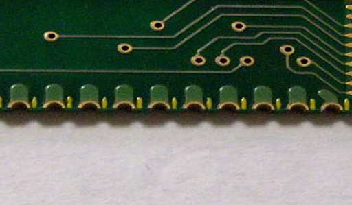
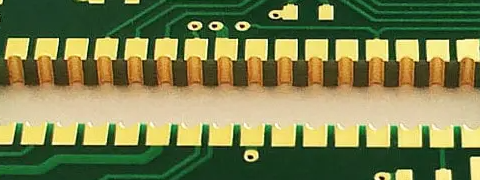
Printed Circuit Board (PCB) edge plating, also known as border plating or castellation, is a specialized manufacturing technique that involves depositing conductive metal, typically copper, along the perimeter edges of a PCB. This process creates continuous electrical connections between the top, bottom, and side surfaces of the board, enabling numerous functional and mechanical advantages in modern electronic designs.
Edge plating has become increasingly important in contemporary electronics as devices demand higher reliability, better electromagnetic compatibility (EMC), and more robust mechanical connections. From consumer electronics to aerospace applications, PCB edge plating serves critical functions that simple through-hole vias or surface mount connections cannot adequately provide.
This article will explore the technical aspects, manufacturing processes, design considerations, and various applications of PCB edge plating, providing engineers and designers with comprehensive knowledge about this important PCB feature.
Technical Specifications and Standards
Materials Used in Edge Plating
The primary material used for PCB edge plating is copper, typically electroplated to thicknesses ranging from 0.0005″ to 0.0014″ (12-35 μm). After copper deposition, the plating is often finished with additional coatings:
- Nickel: Provides a barrier layer (3-5 μm typical) preventing copper diffusion
- Gold: Offers excellent conductivity and corrosion resistance (0.05-0.10 μm)
- Tin: A cost-effective alternative to gold (3-8 μm)
- Silver: Used in specialized high-frequency applications
Industry Standards
Several industry standards govern PCB edge plating specifications:
- IPC-6012: Qualification and Performance Specification for Rigid PCBs
- Class 1: General electronic products
- Class 2: Dedicated service electronic products
- Class 3: High-reliability electronic products
- IPC-A-600: Acceptability of Printed Boards
- Defines acceptable edge plating coverage and quality
- IEC-62326: Printed board standards including edge connection requirements
Key Parameters
Typical edge plating specifications include:
- Plating thickness: 20-35 μm copper minimum
- Edge coverage: Must extend fully from top to bottom surface
- Surface roughness: < 1.5 μm for reliable contact
- Adhesion strength: > 1.0 N/mm (peel test)
Manufacturing Process
Step 1: Panel Design and Preparation
The edge plating process begins at the panel design stage:
- Routing/Milling: The PCB outline is roughed out, leaving about 0.5mm excess material
- Deburring: Mechanical removal of rough edges and debris
- Cleaning: Chemical and mechanical cleaning to ensure proper adhesion
Step 2: Electroless Copper Deposition
- Catalyst Application: Palladium-based catalyst prepares surfaces for copper
- Electroless Copper: 0.3-0.5 μm copper layer deposited chemically
Step 3: Dry Film Resist Application
- Lamination: Photosensitive dry film applied to panel surfaces
- Exposure: UV light exposes pattern for edge plating
- Development: Unwanted resist is removed, exposing copper areas
Step 4: Electrolytic Copper Plating
- Panel Setup: Special fixtures ensure edge coverage
- Copper Plating: 20-35 μm copper deposited via electrolytic process
- Optional Layers: Nickel and/or gold applied as required
Step 5: Final Processing
- Resist Stripping: Removal of dry film resist
- Etching: Removal of unwanted copper
- Final Routing: Precise board outline cutting
- Inspection: Automated optical inspection (AOI) and manual checks
Design Considerations
Electrical Design Factors
- Current Carrying Capacity:
- 1 oz copper (35 μm): ~3A per linear mm of edge
- 2 oz copper (70 μm): ~5A per linear mm
- Impedance Control:
- Critical for high-speed designs
- Requires precise plating thickness control
- Typical tolerance: ±10% of target impedance
- Grounding Strategies:
- Full perimeter grounding for EMI shielding
- Segmented grounding for mixed-signal boards
Mechanical Design Factors
- Board Thickness:
- Standard range: 0.4mm to 3.2mm
- Optimal for edge plating: 1.0mm to 2.4mm
- Edge Chamfering:
- Typically 30° or 45° angles
- Improves connector mating and plating uniformity
- Tolerances:
- Plating position: ±0.1mm
- Board outline: ±0.15mm
- Plating thickness: ±5μm
DFM Guidelines
- Minimum Clearance:
- 0.5mm from edge to nearest trace
- 1.0mm from edge to component
- Plating Extensions:
- Extend plating 0.3mm beyond board edge
- Ensures complete coverage after final routing
- Panelization:
- Include 3-5mm spacing between boards
- Use breakaway tabs or V-grooves
Applications of PCB Edge Plating
EMI Shielding
Edge plating creates a continuous Faraday cage when combined with ground planes:
- Reduces radiated emissions by 10-15dB typically
- Improves immunity to external interference
- Essential for FCC/CE compliance in many products
Edge Connectors
Provides reliable board-to-board connections:
- Card edge connectors (PCIe, ISA, etc.)
- Daughterboard connections
- Backplane systems
High-Current Applications
Distributes current flow across entire board edge:
- Power distribution systems
- High-power LED arrays
- Motor control boards
Harsh Environments
Enhanced protection against:
- Moisture ingress
- Chemical exposure
- Mechanical stress
RF/Microwave Circuits
Controls impedance at board edges:
- Antenna connections
- Radar systems
- 5G infrastructure
Quality Control and Testing
Visual Inspection
- Coverage Check: 100% edge coverage required
- Uniformity: Consistent plating thickness
- Adhesion: No peeling or blistering
Electrical Tests
- Continuity Testing: Verify electrical connection
- Resistance Measurement: < 10mΩ per inch typical
- Hi-Pot Testing: 500V-1000V dielectric withstand
Environmental Tests
- Thermal Cycling: -40°C to +125°C, 100+ cycles
- Humidity Testing: 85°C/85% RH, 1000 hours
- Salt Spray: 96 hours for harsh environments
Common Challenges and Solutions
Plating Uniformity Issues
Problem: Inconsistent plating thickness along edges
Solutions:
- Optimize panel orientation in plating tank
- Use auxiliary cathodes
- Adjust current density (typically 15-25 ASF)
Adhesion Problems
Problem: Plating peeling from substrate
Solutions:
- Improve surface preparation (chemical and mechanical)
- Optimize electroless copper process
- Consider alternative adhesion promoters
Copper Wrap-Around
Problem: Excessive copper on board sides
Solutions:
- Fine-tune dry film application
- Adjust exposure and development parameters
- Implement secondary etching if needed
Future Trends in Edge Plating Technology
Advanced Materials
- Graphene-enhanced plating: For higher conductivity
- Nanocomposite coatings: Improved wear resistance
Process Innovations
- Laser-assisted plating: For precise area control
- Additive manufacturing: Direct metal deposition
Design Integration
- 3D packaging: Edge plating for stacked dies
- Flex-rigid transitions: Continuous plating across materials
Conclusion
PCB edge plating represents a critical technology in modern electronics manufacturing, offering unique solutions for electrical connectivity, mechanical robustness, and electromagnetic compatibility. As electronic devices continue to evolve toward higher frequencies, greater power densities, and more compact form factors, the importance of properly designed and manufactured edge plating will only increase.
By understanding the technical specifications, manufacturing processes, design considerations, and quality control measures outlined in this article, engineers can effectively incorporate edge plating into their PCB designs to achieve superior performance and reliability. Future advancements in materials and processes promise to further expand the capabilities and applications of this essential PCB feature.
For designers working on cutting-edge electronics, mastering PCB edge plating techniques is no longer optional—it’s a necessary skill for creating reliable, high-performance products in an increasingly connected and demanding technological landscape.