The Comprehensive Guide to Patches in PCB Design and Manufacturing
Introduction to PCB Patches
Printed Circuit Board (PCB) patches represent a specialized and increasingly important aspect of modern electronics manufacturing. These small, often overlooked components play critical roles in circuit repair, modification, and even in the initial design phase of electronic devices. A PCB patch can be defined as a localized modification or addition to an existing printed circuit board, typically implemented to correct design flaws, update functionality, or repair damaged circuits without requiring complete board replacement.
In today’s fast-paced electronics industry where time-to-market pressures are intense and design iterations occur rapidly, the ability to implement quick, reliable patches has become an essential skill for PCB designers and manufacturers. This comprehensive guide explores the various types of PCB patches, their applications, implementation techniques, and best practices for effective patching in professional PCB environments.
Types of PCB Patches
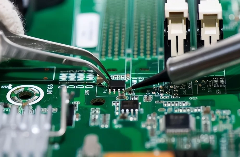
1. Conductive Patches (Copper Patches)
Conductive patches are the most common type used in PCB repair and modification. These involve adding or replacing copper traces to either repair broken connections or create new ones. Copper patches can be implemented through several methods:
- Bodge Wires: Thin insulated wires manually soldered to connect points
- Copper Foil Patches: Adhesive-backed copper tape cut to shape
- Conductive Ink Patches: Printed conductive traces using special inks
- Solder Bridges: Carefully constructed solder connections between points
The choice among these methods depends on factors like current requirements, space constraints, and the desired permanence of the repair.
2. Insulative Patches
Insulative patches serve the opposite purpose of conductive ones—they’re used to isolate or protect areas of a PCB:
- Kapton Tape Applications: High-temperature resistant polyimide film
- Conformal Coating Patches: Localized application of protective coatings
- Solder Mask Patches: UV-curable solder mask for covering exposed copper
- Epoxy Patches: Structural reinforcement for damaged board areas
These patches are particularly valuable in high-voltage applications or environments where electrical isolation is critical.
3. Component Patches
Sometimes patches involve adding or replacing components:
- Surface-Mount Component Additions: Adding small SMD parts to existing pads
- Through-Hole Modifications: Adding components to newly drilled holes
- Stacked Component Solutions: Vertical integration when board space is limited
- Adapter Patches: Small sub-boards that interface between existing components
Component patches are often used for last-minute design changes or feature additions.
4. Structural Patches
These address physical damage to the PCB substrate:
- Fiberglass Reinforcement Patches: For cracked or delaminated areas
- Edge Repair Patches: For damaged board edges or mounting holes
- Via Repair Patches: Specialized solutions for damaged plated through-holes
Applications of PCB Patches
1. Design Error Correction
Despite rigorous design and verification processes, errors sometimes only become apparent during prototyping or even full production. Common design errors that patches can address include:
- Incorrect trace routing
- Missing connections
- Wrong component footprints
- Power distribution issues
- Signal integrity problems
Patches allow for rapid correction without the time and cost of spinning a new board revision.
2. Field Repairs and Maintenance
In field service scenarios, complete board replacement may be impractical or cost-prohibitive. Patches enable:
- On-site repair of damaged equipment
- Extension of product service life
- Temporary fixes while awaiting replacement parts
- Legacy system support when original components are obsolete
3. Prototype Modification
During product development, patches facilitate:
- Rapid design iteration testing
- Feature additions between prototype versions
- Performance optimization tweaks
- Alternative configuration testing
4. Product Upgrades and Customization
Patches can serve as an implementation method for:
- Firmware update support circuits
- Feature enablement/disablement
- Region-specific modifications
- Customer-specific customizations
PCB Patch Implementation Techniques
1. Manual Patching Methods
Traditional hand-applied patching remains valuable for low-volume or quick-turn needs:
- Precision Soldering: Requires skilled technicians and proper tools
- Micro-Drilling: For creating new via connections
- Trace Cutting: Isolating problematic circuit sections
- Conformal Coating Removal: For accessing underlying circuits
2. Semi-Automated Patching Solutions
Bridging the gap between manual and full automation:
- Conductive Ink Printing: Direct-write systems for trace repair
- Laser-Assisted Deposition: Precise material addition
- Micro-Dispensing: Accurate adhesive or epoxy application
- Automated Optical Inspection (AOI) Guided Repair: Computer-assisted patching
3. Design-Level Patching
Incorporating patching considerations into original PCB design:
- Test Points and Debug Headers: Intentional access points
- Programmable Logic: For software-configurable patches
- Modular Sub-Sections: Easily replaceable circuit blocks
- Expansion Interfaces: Designed-in connection points
Best Practices for Effective PCB Patching
1. Pre-Patch Assessment
- Thoroughly analyze the root cause of the issue
- Evaluate all potential patching options
- Consider long-term reliability implications
- Document the original fault and proposed solution
2. Material Selection
- Match substrate materials for thermal expansion compatibility
- Select adhesives with appropriate curing requirements
- Choose conductors with compatible resistivity
- Consider chemical compatibility with existing board materials
3. Process Control
- Maintain clean work environments
- Control temperature and humidity during patching
- Implement proper curing/baking processes
- Follow ESD protection protocols
4. Quality Verification
- Electrical testing of patched connections
- Mechanical stress testing where applicable
- Environmental testing for harsh condition boards
- Long-term reliability assessment
Advanced Patching Technologies
1. Nano-Material Patches
Emerging technologies utilizing:
- Carbon nanotube-based conductors
- Graphene-enhanced adhesives
- Nano-particle conductive inks
- Self-healing conductive materials
2. 3D Printed Electronics Patches
Additive manufacturing approaches:
- Direct trace printing on existing boards
- Three-dimensional conductive structures
- Custom dielectric deposition
- Integrated component placement
3. Smart Patches
Intelligent patching solutions featuring:
- Embedded diagnostic capabilities
- Self-monitoring connections
- Programmable interface patches
- Wireless updateable patch circuits
Challenges and Limitations of PCB Patching
While patching offers numerous benefits, several challenges exist:
- Signal Integrity Concerns: Patches may introduce impedance mismatches or noise
- Thermal Management Issues: Altered heat dissipation paths
- Mechanical Reliability: Potential weak points in the assembly
- Aesthetic Considerations: Important for consumer products
- Certification Impacts: May require re-certification of safety-critical devices
- Documentation Burden: Must accurately reflect as-built configurations
Future Trends in PCB Patching Technology
The field of PCB patching continues to evolve with several promising developments:
- AI-Assisted Patching: Machine learning algorithms that suggest optimal patch solutions
- Robotic Micro-Patching: Automated systems for high-precision repairs
- Bio-Compatible Patches: For medical electronics applications
- Transient Electronics: Temporary patches that dissolve after serving their purpose
- Quantum Dot Patches: Novel conductive materials with unique properties
Conclusion
PCB patches represent a vital toolkit in the electronics manufacturing and maintenance ecosystem. From simple bodge wires to sophisticated nano-material solutions, patching technologies continue to evolve alongside the PCBs they repair and modify. As electronic devices become more complex and miniaturized, the importance of reliable, high-quality patching solutions only grows.
Understanding the various types of patches, their appropriate applications, and implementation best practices enables engineers and technicians to extend product lifecycles, reduce electronic waste, and maintain systems in ways that would otherwise be impractical or impossible. While patching should never replace proper design practices, it remains an essential skill in the PCB professional’s repertoire.
As we look to the future, advancements in materials science, manufacturing technologies, and artificial intelligence promise to further revolutionize what’s possible in PCB patching, opening new possibilities for repair, modification, and even enhancement of electronic systems at the most fundamental level.