PCB Tombstoning: Causes, Prevention, and Solutions in Surface Mount Technology
Introduction to Tombstoning in PCB Assembly
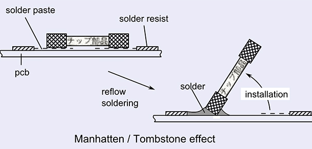
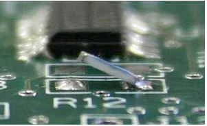
Printed Circuit Board (PCB) tombstoning, also known as the “Manhattan effect,” “drawbridging,” or “chip-standing,” is a common defect in surface mount technology (SMT) assembly that occurs when a passive component (typically a resistor or capacitor) stands up on one end during the reflow soldering process. This phenomenon creates an open circuit as only one termination makes contact with the pad, while the other lifts away from the PCB surface, resembling a tombstone – hence the name.
Tombstoning represents a significant quality control challenge in modern electronics manufacturing, particularly as components continue to shrink in size and PCBs become more densely populated. The defect not only impacts production yields but can also lead to field failures if undetected during inspection. Understanding the root causes of tombstoning and implementing effective prevention strategies is essential for maintaining high-quality SMT assembly processes.
This comprehensive article examines the physics behind tombstoning, analyzes its primary causes, explores prevention techniques, and discusses solutions for addressing tombstoned components in production environments. By addressing tombstoning systematically, manufacturers can significantly improve their assembly yields and product reliability.
The Physics Behind Tombstoning
To effectively prevent tombstoning, it’s crucial to understand the physical forces that cause components to stand up during reflow soldering. Tombstoning occurs due to an imbalance in the wetting forces acting on the component’s terminations during the critical liquidus phase of solder melting.
When solder paste melts during reflow, surface tension creates a vertical force component that pulls upward on the component termination. Under normal conditions, these forces balance each other when:
1) Both solder joints melt simultaneously
2) The solder volumes are equal
3) The pad sizes are symmetrical
4) The thermal conditions are uniform
When any of these conditions are not met, an imbalance occurs. If one solder joint melts before the other or develops greater surface tension, the stronger force can literally pull the component upright. The moment when the solder transitions from paste to liquid (known as the “liquidus phase”) is particularly critical because this is when surface tension forces are highest.
Smaller components (especially 0201, 01005, and smaller metric equivalents) are more susceptible to tombstoning because:
1) Their lighter mass offers less resistance to the surface tension forces
2) The distance between terminations is shorter, allowing smaller force imbalances to create rotation
3) Their smaller size makes them more sensitive to process variations
Component geometry also plays a role. Rectangular chip components have more surface area for solder wetting compared to round components, which affects how forces are distributed during reflow.
Primary Causes of PCB Tombstoning
1. Pad Design and Layout Imbalances
One of the most common root causes of tombstoning is asymmetrical pad design or layout. Issues include:
- Unequal pad sizes: When one pad has significantly more copper area than its counterpart, it can create thermal imbalances during reflow. The larger pad acts as a heat sink, causing the solder on that side to melt later than the smaller pad.
- Different trace connections: If one pad connects to a large copper pour or thick trace while the other connects to a thin trace, the thermal mass difference can create uneven heating.
- Non-symmetrical component placement: Components placed too close to large thermal masses (like ground planes or heatsinks) may experience uneven heating.
- Incorrect pad spacing: If the gap between pads doesn’t precisely match the component’s termination spacing, it can create tension during reflow.
2. Solder Paste Deposition Issues
Variations in solder paste application can create the force imbalances that lead to tombstoning:
- Uneven stencil aperture sizes: If the stencil openings for paired pads aren’t identical, they’ll deposit different solder volumes.
- Stencil misalignment: Off-center paste deposition can put more paste on one pad than the other.
- Solder paste slump: Excessive slump before reflow can redistribute paste unevenly.
- Printing defects: Wiping issues, stencil clogging, or poor gasketting can create paste volume disparities.
3. Component Variations
While less common than process-related causes, component characteristics can contribute to tombstoning:
- Termination finish differences: Inconsistent metallization on component ends can affect wetting behavior.
- Dimensional tolerances: Variations in component length or termination placement can create imbalances.
- Warpage: Components that aren’t perfectly flat may have one termination slightly elevated.
4. Reflow Profile Issues
The temperature profile during reflow significantly impacts tombstoning rates:
- Excessive ramp rates: Fast heating can exacerbate thermal imbalances between pads.
- Uneven heating: Poor oven uniformity or board orientation can create side-to-side temperature differences.
- Peak temperature too high: Excessive heat can increase surface tension forces.
- Time above liquidus (TAL): Both insufficient and excessive TAL can contribute to tombstoning.
5. Environmental Factors
- Oxidation: Contaminated or oxidized pads or component terminations can inhibit proper wetting.
- Moisture: Absorbed moisture in components can create outgassing during reflow, affecting solder flow.
- Storage conditions: Improper component storage can degrade termination finishes over time.
Prevention Strategies for PCB Tombstoning
1. Optimized Pad Design
Implementing proper pad geometries is the first line of defense against tombstoning:
- Symmetrical pad sizes: Ensure both pads have identical copper areas and thermal characteristics.
- Balanced thermal relief: When one pad must connect to a large copper area, use thermal relief patterns to balance heat dissipation.
- Proper pad spacing: Follow component manufacturer recommendations for pad-to-pad spacing.
- Pad size ratios: For problem components, slightly reducing the size of the hotter pad can help balance melting times.
2. Solder Paste Management
- Stencil design optimization: Ensure stencil apertures are symmetrical and properly sized for the components.
- Paste volume control: Maintain consistent paste deposition through proper stencil maintenance and printing processes.
- Paste selection: Consider low-tombstoning solder pastes with appropriate metal content and flux chemistry.
3. Reflow Profile Optimization
Developing the right thermal profile is critical:
- Controlled ramp rates: Typically 1-3°C/second to minimize thermal gradients.
- Proper preheat: Adequate preheat helps activate flux and reduce thermal shock.
- Balanced heating: Ensure even heating across the PCB through proper oven setup and board orientation.
- Peak temperature control: Stay within recommended ranges for both components and solder paste.
4. Process Controls
- Component placement accuracy: Precise placement ensures proper alignment with pads.
- Moisture sensitive component handling: Follow MSL guidelines to prevent popcorning and outgassing.
- Nitrogen reflow: When possible, using nitrogen atmosphere can improve wetting and reduce oxidation.
5. Design for Manufacturing (DFM) Reviews
Conduct thorough DFM analyses to identify potential tombstoning risks before production:
- Thermal symmetry analysis: Evaluate copper distribution around sensitive components.
- Component orientation: Align components to minimize thermal gradients during reflow.
- Board layout: Avoid placing small passives near large thermal masses or board edges.
Solutions for Addressing Tombstoned Components
Despite best prevention efforts, tombstoning may still occur. Effective solutions include:
1. Detection Methods
- Automated Optical Inspection (AOI): High-resolution cameras can identify standing components.
- 3D solder paste inspection (SPI): Can detect paste volume imbalances that may lead to tombstoning.
- X-ray inspection: Useful for hidden joints or complex assemblies.
2. Rework Techniques
- Hot air rework: Carefully reflow the tombstoned component while applying gentle pressure.
- Hand soldering: For accessible components, skilled technicians can resolder the lifted end.
- Solder addition: Sometimes adding a small amount of solder can help re-establish connection.
3. Process Adjustment
When tombstoning defects are detected:
- Stop the line: Investigate root causes before continuing production.
- Profile adjustment: Modify reflow parameters based on defect analysis.
- Stencil verification: Check for clogging or misalignment issues.
4. Design Modifications
For persistent tombstoning issues:
- Pad geometry revisions: Adjust pad sizes or shapes to balance thermal characteristics.
- Solder mask adjustments: Changing solder mask openings can affect heat transfer.
- Component substitutions: In some cases, alternative components may be less prone to tombstoning.
Advanced Considerations in Tombstoning Prevention
As components continue to shrink, new challenges emerge:
1. Ultra-Small Components (01005 and smaller)
These tiny components require exceptional process control:
- Laser-cut stencils: For precise aperture definition.
- High-accuracy placement: ±15μm or better placement capability.
- Enhanced profile control: Tight temperature uniformity requirements.
2. Mixed Technology Boards
Combining through-hole and SMT components creates thermal challenges:
- Selective heating strategies: May require special conveyor setups or zone controls.
- Component sequencing: Place temperature-sensitive components last.
3. Low-Temperature Solders
New solder alloys for temperature-sensitive components:
- Different wetting characteristics: Require profile adjustments.
- Reduced surface tension: Can help minimize tombstoning forces.
4. High-Density Interconnect (HDI) PCBs
Dense layouts create thermal management challenges:
- Microvia effects: Can create localized heating differences.
- Thin dielectrics: Affect heat distribution across the board.
Conclusion
PCB tombstoning remains a significant challenge in surface mount assembly, particularly as electronic components continue to decrease in size while complexity increases. By understanding the fundamental physics behind tombstoning and systematically addressing its root causes—through optimized pad design, precise solder paste application, controlled reflow profiling, and rigorous process controls—manufacturers can dramatically reduce tombstoning defects.
Prevention remains far more cost-effective than detection and rework, making DFM analyses and process validation critical steps in new product introduction. As the industry moves toward even smaller components and more complex assemblies, continued attention to tombstoning mechanisms and innovative prevention strategies will be essential for maintaining high yields and reliable products.
Through a combination of good design practices, precise process control, and continuous monitoring, tombstoning can be effectively managed, ensuring the production of reliable, high-quality electronic assemblies in even the most demanding applications.