Advanced PCBA Assembly Techniques for Enhanced Reliability
Key Takeaways
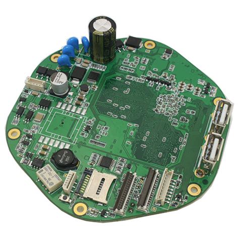
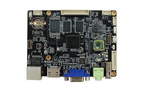
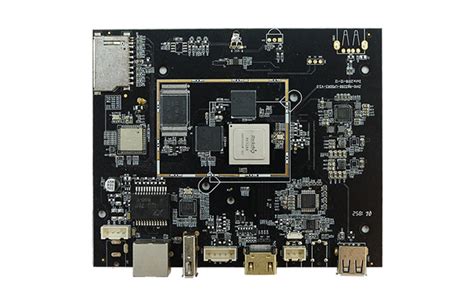
Modern PCBA processes rely on precision engineering and rigorous quality protocols to ensure robust electronic systems. At the core of PCB assembly advancements are innovations in precision soldering, which minimize defects like cold joints or bridging, directly enhancing long-term reliability. Equally critical is automated component placement, where high-speed machines achieve micron-level accuracy, reducing human error and optimizing production scalability.
To maintain consistency, manufacturers integrate automated optical inspection (AOI) and X-ray testing into workflows, identifying latent flaws in solder joints or component alignment. Thermal management strategies, such as heat-resistant substrates and thermal interface materials, mitigate stress from operational temperatures, extending product lifespans. Material selection also plays a pivotal role—high-grade substrates and lead-free solder alloys ensure compliance with environmental standards while improving durability.
Finally, conformal coating techniques provide an additional layer of protection against moisture, dust, and chemical exposure, safeguarding PCBA integrity in harsh environments. By harmonizing these techniques, engineers achieve a balance between performance, reliability, and cost-efficiency in modern electronics manufacturing.
Precision Soldering in PCBA Assembly
Precision soldering forms the backbone of reliable PCB assembly, ensuring robust electrical connections and mechanical stability in PCBA manufacturing. Modern techniques leverage lead-free solder alloys with melting points optimized for thermal profiles ranging from 217°C to 250°C, balancing environmental compliance and performance. Advanced systems employ automated optical inspection (AOI) to detect micro-level defects like cold joints or bridging, reducing failure rates by up to 40% compared to manual methods.
A critical advancement lies in laser soldering, which achieves micron-level accuracy for high-density interconnects (HDI) in compact devices. This method minimizes heat dispersion, preserving sensitive components such as ball grid arrays (BGAs). For mixed-technology boards, selective soldering targets specific areas, avoiding thermal stress on pre-mounted surface-mount devices (SMDs).
| Soldering Method | Temperature Range (°C) | Key Application |
|---|---|---|
| Reflow Soldering | 220–250 | SMDs in high-volume production |
| Wave Soldering | 260–280 | Through-hole components |
| Laser Soldering | 200–220 | Precision microelectronics |
| Selective Soldering | 250–270 | Hybrid component boards |
To ensure consistency, PCBA manufacturers implement closed-loop thermal control systems, maintaining ±1.5°C tolerance during solder reflow. This precision prevents tin whiskers and intermetallic compound formation, both critical for long-term reliability in harsh environments. Pairing these techniques with flux chemistry optimization further enhances wetting properties, ensuring void rates below 5% in X-ray inspections. As component miniaturization accelerates, precision soldering remains pivotal in achieving the durability standards demanded by aerospace, automotive, and medical electronics sectors.
Automated Component Placement Technology
Modern PCB assembly processes rely heavily on robotic placement systems to achieve micron-level accuracy in component positioning. These systems integrate vision alignment technologies and high-speed pick-and-place mechanisms to handle components ranging from 0201 resistors to complex BGAs (Ball Grid Arrays). By leveraging machine learning algorithms, automated systems dynamically adjust placement parameters based on real-time feedback, minimizing misalignment risks that could compromise PCBA reliability.
A critical advancement lies in multi-head placement architectures, which enable simultaneous handling of diverse components while maintaining throughput rates exceeding 50,000 placements per hour. This precision reduces solder bridging and tombstoning defects during subsequent reflow stages, directly enhancing end-product durability. For high-density interconnect (HDI) boards, automated systems employ laser-assisted calibration to navigate ultra-fine pitch layouts, ensuring consistent contact pad alignment even under thermal stress.
Transitioning seamlessly into quality control workflows, these technologies feed placement data into AOI (Automated Optical Inspection) systems, creating a closed-loop verification process. Such integration not only streamlines PCB assembly timelines but also elevates traceability standards—a foundational requirement for aerospace, medical, and automotive applications where PCBA failure is not an option.
Quality Control Strategies for PCB Reliability
Implementing robust quality control protocols is critical in PCB assembly processes to ensure long-term reliability of PCBA-based systems. Modern strategies combine automated optical inspection (AOI) with X-ray fluorescence (XRF) testing to detect solder joint defects, component misalignment, and material inconsistencies at micron-level precision. For high-density boards, electrical testing validates circuit continuity, while thermal cycling simulates real-world stress to identify potential failure points.
"Adopting a tiered inspection approach — combining automated systems with manual sampling — reduces defect escape rates by up to 98% in complex PCBA projects."
Advanced manufacturers now integrate statistical process control (SPC) tools to monitor PCB assembly parameters like reflow oven temperature profiles and solder paste deposition volumes. This data-driven method enables real-time adjustments, maintaining process capability indices (CpK) above 1.67 for critical characteristics. Cross-functional teams also employ failure mode and effects analysis (FMEA) during design-for-manufacturing (DFM) reviews to preempt reliability risks in PCBA layouts.
For mission-critical applications, ion chromatography tests verify post-assembly cleanliness, preventing electrochemical migration that could compromise PCB insulation resistance. These layered strategies collectively enhance mean time between failures (MTBF) while meeting IPC-A-610 Class 3 standards for harsh-environment electronics.
Thermal Management in Circuit Board Assembly
Effective thermal management in PCB assembly is critical for maintaining long-term reliability and preventing premature failure in electronic systems. As component density increases in modern PCBA designs, managing heat dissipation becomes a complex challenge requiring multi-layered solutions. Engineers prioritize thermal vias and copper pours to create efficient heat pathways, while selecting substrates with high glass transition temperatures (Tg) to withstand elevated operating conditions.
Advanced PCB assembly processes now integrate phase-change materials and thermal interface compounds between heat-sensitive components and heatsinks, optimizing conductive cooling. For high-power applications, active cooling systems—such as embedded micro-fans or liquid cooling channels—are increasingly paired with PCBA layouts to achieve balanced thermal distribution. Automated infrared inspection during manufacturing ensures proper solder joint integrity, which directly impacts heat transfer efficiency.
Proactive thermal simulation during the design phase helps identify hotspots before prototyping, enabling adjustments to trace widths or component placement. This approach not only enhances thermal management but also aligns with broader quality control strategies outlined in earlier sections, ensuring cohesive reliability across all stages of production.
Advanced Inspection Methods for PCBA
Modern PCB assembly processes demand rigorous quality assurance to ensure long-term reliability. Automated optical inspection (AOI) systems now utilize high-resolution cameras and machine learning algorithms to detect microscopic defects in PCBA, such as solder bridging, component misalignment, or missing parts. Complementing these visual systems, X-ray inspection penetrates layered structures to identify voids in ball grid array (BGA) joints or hidden cracks in multilayer boards—critical for aerospace and medical devices where failure is not an option.
For real-time performance validation, infrared thermal imaging monitors heat distribution during functional testing, flagging hotspots that indicate poor solder connections or overloaded circuits. Additionally, in-circuit test (ICT) fixtures validate electrical continuity and component functionality at speeds exceeding 10,000 test points per minute. When combined with statistical process control (SPC) analytics, these methods create a闭环 feedback loop, enabling rapid adjustments in PCB assembly workflows. By integrating these advanced inspection layers, manufacturers reduce field failure rates by up to 40% while maintaining compliance with IPC-A-610 and J-STD-001 standards—proactively addressing defects before they compromise PCBA reliability.
Material Selection for Durable Electronics
The longevity of electronic systems hinges on PCB assembly processes that prioritize strategic material selection. Engineers must evaluate substrate materials, conductive traces, and solder alloys for their thermal, mechanical, and environmental resistance properties. High-performance substrates like FR-4 with halogen-free formulations or polyimide laminates offer enhanced thermal stability, critical for applications exposed to temperature fluctuations or prolonged operational stress.
In PCBA, copper weight and surface finishes (e.g., ENIG or immersion silver) directly influence conductivity and corrosion resistance. For harsh environments, conformal coatings such as acrylic or silicone-based compounds provide moisture and chemical protection, extending the lifespan of assembled boards. Advanced solder alloys, including SAC305 (Sn96.5/Ag3.0/Cu0.5), balance melting points with mechanical strength to withstand vibration and thermal cycling.
Material compatibility with automated PCB assembly workflows is equally vital. Components with mismatched coefficients of thermal expansion (CTE) risk delamination or solder joint fractures during reflow. By integrating CTE-matched materials and leveraging simulation tools, manufacturers preempt failure modes, ensuring reliability aligns with industry standards like IPC-6012. This systematic approach to material science fortifies PCBA durability without compromising precision or scalability in high-volume production.
SMT Process Optimization Techniques
Effective SMT process optimization ensures consistent quality in PCB assembly by addressing critical variables in surface-mount technology workflows. Precision-controlled solder paste deposition forms the foundation, with modern PCBA lines utilizing automated optical inspection (AOI) systems to verify stencil alignment and paste volume accuracy. Advanced pick-and-place machines now achieve sub-10-micron positioning repeatability, enabling error-free mounting of 0201-size components and micro-BGA packages.
Thermal profiling during reflow soldering has evolved with machine learning algorithms that dynamically adjust zone temperatures based on real-time board thickness and component density data. This data-driven approach minimizes thermal stress while maintaining proper intermetallic bonding. Additionally, nitrogen-enclosed reflow ovens reduce oxidation risks, particularly for high-density interconnect (HDI) PCB assemblies.
To further optimize SMT throughput, engineers employ closed-loop feedback systems that correlate process parameters with post-assembly test results. By analyzing X-ray inspection data and functional test outcomes, production teams can fine-tune placement pressure, solder paste alloys, and conveyor speed settings. These refinements collectively enhance PCBA reliability while reducing defect rates below 50 ppm in optimized manufacturing environments.
Conformal Coating for Enhanced Protection
In PCB assembly, conformal coating serves as a critical safeguard against environmental stressors that compromise electronic reliability. This ultra-thin protective layer, applied post-PCBA manufacturing, shields circuits from moisture, chemical exposure, and mechanical abrasion while maintaining electrical functionality. Advanced formulations—including acrylic, silicone, and urethane-based coatings—are selected based on operational demands, such as thermal cycling resistance or dielectric performance.
Automated spray systems ensure uniform coverage across complex board geometries, minimizing voids that could expose sensitive components. For high-precision PCBA applications, selective coating techniques target specific areas, preserving connector accessibility and heat dissipation pathways. Post-application inspection employs ultraviolet (UV) tracer dyes or automated optical inspection (AOI) to verify coating integrity, addressing defects like pinholes or uneven edges before final testing.
By integrating conformal coating into PCB assembly workflows, manufacturers reduce failure rates in harsh environments—from industrial machinery to automotive systems. This process not only extends product lifespans but also aligns with industry standards for corrosion resistance and contaminant mitigation, ensuring consistent performance across temperature fluctuations and operational cycles.
Conclusion
As the culmination of modern manufacturing methodologies, PCB assembly processes now integrate precision-engineered solutions that address both performance and longevity challenges. The evolution of PCBA techniques—from laser-aligned soldering to AI-driven inspection systems—demonstrates how technological advancements are redefining reliability standards in electronics production. By harmonizing material science innovations with data-centric quality controls, manufacturers achieve unprecedented consistency in high-density interconnect (HDI) boards and mission-critical systems.
Transitioning from design to deployment, thermal optimization protocols and conformal coating applications ensure operational stability across extreme environments, while automated placement technologies minimize human-induced variability. These synergies not only reduce defect rates but also extend product lifecycles, aligning with industry demands for sustainable electronics. For engineers, prioritizing traceability in PCB assembly workflows and adopting predictive maintenance models for PCBA units will remain pivotal in navigating future complexity. Ultimately, the integration of these strategies fosters resilient ecosystems where reliability is no longer an aspiration but a measurable outcome.
FAQs
What distinguishes pcb assembly from pcba in manufacturing?
PCB assembly refers to the process of populating a bare circuit board with components, while PCBA (Printed Circuit Board Assembly) denotes the completed, functional unit ready for integration into electronic devices. Modern techniques leverage automated placement and precision soldering to ensure optimal performance.
How does thermal management affect pcba reliability?
Effective thermal management prevents component degradation by dissipating heat through advanced materials like metal-core substrates or thermal vias. Poor heat control can lead to solder joint failures, reducing the lifespan of electronic systems.
What quality control methods ensure durable pcb assembly?
Automated Optical Inspection (AOI) and X-ray imaging detect micro-defects in solder joints, while in-circuit testing validates electrical functionality. Combining these with conformal coating enhances protection against environmental stressors.
Why is material selection critical for pcba longevity?
High-grade substrates, lead-free solder alloys, and moisture-resistant laminates mitigate wear from thermal cycling and humidity. Selecting components rated for extended temperature ranges further improves durability in harsh operating conditions.
Explore Professional PCBA Solutions
For tailored pcb assembly services integrating these advanced techniques, please click here to consult our engineering team.