Efficient Turnkey Prototype Assembly for Faster Market Entry
Key Takeaways
Modern product development cycles demand integrated approaches to PCB assembly and PCBA processes, particularly when accelerating time-to-market. Turnkey prototype assembly services eliminate fragmented workflows by combining design validation, component sourcing, and precision manufacturing into a unified system. This holistic methodology reduces iterative delays, with studies showing a 40-60% reduction in development phases compared to traditional siloed approaches.
"The synergy between PCB assembly and rapid prototyping creates a feedback loop where design improvements directly inform manufacturing readiness," notes a leading hardware engineer at a Fortune 500 tech firm.
| Traditional Process | Turnkey Prototype Assembly |
|---|---|
| Multi-vendor coordination | Single-point accountability |
| 12-16 week lead times | 4-6 week execution cycles |
| Inconsistent quality control | ISO-certified PCBA standards |
For optimal results, prioritize partners offering real-time design-for-manufacturability (DFM) feedback during PCB assembly. This proactive strategy identifies potential production bottlenecks before prototyping begins, ensuring market-ready iterations. Additionally, scalable PCBA solutions enable seamless transitions from low-volume batches to mass production, maintaining component consistency across phases.
Tip: When evaluating turnkey services, verify their capability to handle both high-mix, low-volume prototype builds and future scaling demands. This dual-capacity alignment ensures continuity as products move from validation to commercialization.
Streamlining Product Development With Turnkey Prototypes
Modern product development demands seamless integration of design, testing, and manufacturing phases. PCB assembly (PCBA) services form the backbone of turnkey prototyping solutions, enabling teams to bridge the gap between concept validation and production readiness. By leveraging end-to-end PCBA workflows, engineers gain access to synchronized processes—from component sourcing to functional testing—that eliminate fragmented vendor relationships and reduce iterative delays.
A key advantage lies in precision manufacturing techniques, where automated PCB assembly systems ensure consistent quality while adhering to tight tolerances. This approach minimizes rework cycles during critical stages like design validation, allowing teams to identify performance gaps early. Integrated PCBA solutions further accelerate timelines by combining rapid prototyping with scalable manufacturing frameworks, ensuring prototypes meet market-ready specifications from the first iteration.
Transitioning between phases becomes effortless as turnkey providers manage logistics, compliance, and quality assurance in parallel. For instance, real-time collaboration between design engineers and PCB assembly experts optimizes layouts for manufacturability, reducing post-prototype adjustments. Such synergy not only shortens development cycles but also creates a foundation for smooth scaling—a strategic advantage in industries where time-to-market dictates competitive success.
Accelerating Market Entry Through Precision Assembly
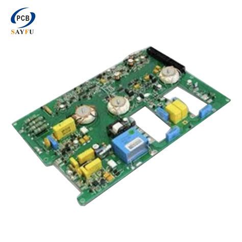
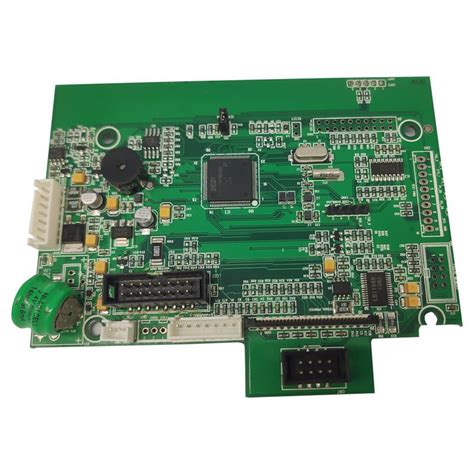
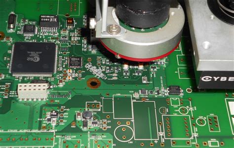
Modern PCB assembly (PCBA) services play a pivotal role in compressing development timelines while maintaining rigorous quality standards. By integrating precision assembly workflows with advanced automation, manufacturers can achieve first-pass success rates exceeding 95%, significantly reducing iterative redesign cycles. This approach ensures critical components—from multilayer PCBA configurations to surface-mount integrations—are optimized for functional validation and environmental stress testing.
Strategic alignment between PCB assembly specialists and engineering teams enables real-time design adjustments, addressing potential manufacturability issues before physical prototyping begins. For instance, automated optical inspection (AOI) systems coupled with 3D solder paste analysis guarantee micron-level accuracy across complex circuit architectures. Such precision not only accelerates functional verification but also creates a seamless pathway for scaling validated prototypes into pilot production.
By leveraging turnkey PCBA solutions, companies eliminate fragmented supply chain dependencies, consolidating tasks like component sourcing, conformal coating, and functional testing under unified quality protocols. This holistic manufacturing strategy reduces time-to-market by 30–45% compared to traditional assembly methods, ensuring prototypes meet both technical specifications and regulatory compliance benchmarks from the outset. The result is a market-ready product that transitions efficiently from validation phases to volume manufacturing without compromising performance or reliability.
End-to-End Prototyping Solutions for Faster Scaling
Modern product development demands integrated workflows that bridge design validation and scalable production. By combining PCB assembly expertise with advanced PCBA processes, manufacturers eliminate fragmented workflows that traditionally delay time-to-market. End-to-end prototyping solutions address this challenge by synchronizing design optimization, component sourcing, and functional testing into a unified framework. For instance, automated design-for-manufacturing (DFM) checks during PCB assembly ensure prototypes meet both performance benchmarks and mass-production readiness criteria, reducing iterative redesign cycles by up to 40%.
The scalability of these systems hinges on seamless transitions between prototyping phases. Advanced PCBA providers leverage modular tooling and standardized interfaces, enabling rapid adjustments to component layouts or material specifications without halting production lines. This agility is critical for industries like IoT and medical devices, where regulatory compliance and component traceability are non-negotiable. By embedding quality control protocols directly into PCB assembly workflows—such as automated optical inspection (AOI) and in-circuit testing (ICT)—teams can validate prototypes against real-world operational conditions while maintaining alignment with future scaling requirements.
Ultimately, the integration of PCBA expertise into prototyping ecosystems creates a foundation for risk-mitigated scaling. From validating thermal management in compact electronics to stress-testing high-frequency signal integrity, end-to-end solutions ensure prototypes evolve into market-ready products without compromising on manufacturability or cost efficiency.
Optimizing Design Validation With Turnkey Services
Effective design validation relies on PCB assembly processes that mirror final production conditions while maintaining flexibility for iterative improvements. Turnkey services bridge the gap between conceptual designs and functional prototypes by integrating PCBA expertise with comprehensive testing protocols. By consolidating component sourcing, assembly, and validation under a single workflow, engineers gain access to real-time performance data, enabling rapid identification of design flaws in power distribution, signal integrity, or thermal management.
Advanced PCB assembly partners utilize automated optical inspection (AOI) and in-circuit testing (ICT) to validate prototypes against industry standards, reducing validation cycles by up to 40%. This approach ensures design-for-manufacturability (DFM) principles are embedded early, minimizing costly revisions during scaling. For instance, PCBA specialists often employ concurrent engineering strategies, where mechanical, electrical, and firmware teams collaborate to troubleshoot cross-disciplinary issues before mass production.
Transitioning seamlessly to the next phase, these optimized validation processes directly support faster iterations, ensuring prototypes meet both technical specifications and market demands. By leveraging turnkey solutions, companies systematically eliminate bottlenecks in design verification, laying the groundwork for reliable product commercialization.
Reducing Time-to-Market via Prototype Assembly Systems
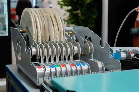
Modern PCB assembly and PCBA processes form the backbone of efficient turnkey prototype systems, enabling businesses to compress development cycles while maintaining rigorous quality standards. By integrating design validation, precision manufacturing, and scalability planning into a unified workflow, these systems eliminate fragmented workflows that traditionally delay progress. Advanced automated optical inspection (AOI) and surface-mount technology (SMT) ensure rapid iteration of functional prototypes, reducing errors that might otherwise require costly redesigns.
A key advantage lies in the seamless coordination between PCB assembly teams and product engineers, which accelerates design-for-manufacturability adjustments. For instance, real-time feedback on PCBA layouts allows immediate corrections to component placement or thermal management, bypassing weeks of back-and-forth revisions. Additionally, turnkey providers leverage pre-vetted supply chains to mitigate material shortages—a common bottleneck in prototype development.
By aligning prototype assembly systems with lean manufacturing principles, companies can shorten the critical path from concept to market-ready product. This approach not only enhances first-pass yield rates but also establishes a foundation for smooth scaling, ensuring that validated prototypes transition effortlessly into mass production without compromising timelines or performance benchmarks.
Seamless Transition From Prototype to Mass Production
Achieving a frictionless shift from prototype development to full-scale manufacturing requires integrated workflows that bridge PCB assembly expertise with scalable production methodologies. Modern PCBA (Printed Circuit Board Assembly) services now incorporate design-for-manufacturability principles during prototyping, ensuring component compatibility and process alignment with high-volume requirements. By leveraging turnkey prototype assembly systems, teams can validate not just product functionality but also manufacturing readiness through standardized testing protocols and material traceability.
At the core of this process lies the synchronization of PCB assembly tolerances across prototype and production phases. Advanced PCBA providers utilize identical equipment and quality controls for both stages, minimizing discrepancies in solder joint integrity or component placement accuracy. This technical alignment reduces post-prototype redesign cycles by up to 40%, directly accelerating time-to-market. Additionally, supply chain integration ensures critical parts remain available at scale, avoiding bottlenecks during ramp-up.
Transition-focused strategies further optimize this journey by embedding failure mode analysis early in prototyping. Teams preemptively address thermal management, signal integrity, and mechanical stress points—factors critical for mass production reliability. With turnkey prototype assembly acting as a bridge, innovators can scale confidently, knowing their validated designs translate seamlessly into market-ready products.
Turnkey Assembly Strategies for Market-Ready Products
Effective turnkey prototype assembly requires harmonizing PCB assembly expertise with scalable manufacturing workflows. By integrating PCBA processes early in product development, teams achieve seamless synchronization between electronic components and mechanical enclosures, eliminating iterative redesign cycles. Advanced PCB assembly systems now incorporate automated optical inspection (AOI) and functional testing protocols, ensuring first-pass success rates exceeding 90% for complex circuit boards.
Strategic partners leverage turnkey workflows to unify design validation, material sourcing, and low-volume production under one roof, compressing timelines by 30–50% compared to fragmented approaches. For IoT devices or embedded systems, optimized PCBA integration addresses thermal management and signal integrity challenges proactively, directly aligning prototypes with mass production requirements. Real-time data sharing between engineering and manufacturing teams further enables rapid iteration of board layouts or component placements without compromising compliance standards.
This holistic strategy not only accelerates market entry but also establishes a foundation for cost-efficient scaling. By standardizing PCB assembly tolerances and testing benchmarks, companies mitigate supply chain risks while maintaining consistency across prototype batches and high-volume orders alike.
Precision Manufacturing for Rapid Prototype Deployment
Modern PCB assembly processes form the backbone of high-velocity prototype development, enabling engineers to bridge design concepts and functional models with unmatched accuracy. By integrating PCBA (Printed Circuit Board Assembly) expertise into turnkey workflows, manufacturers achieve sub-millimeter precision in component placement, solder joint integrity, and functional testing—critical factors for validating complex electronics under real-world conditions. Advanced surface-mount technology (SMT) lines, coupled with automated optical inspection (AOI), ensure first-pass success rates exceeding 98%, eliminating costly rework cycles during PCB assembly phases.
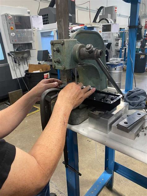
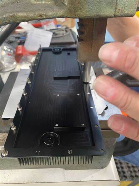
This precision-driven approach extends beyond circuitry, applying laser-calibrated machining and 3D-printed enclosures to create aerospace-grade mechanical prototypes within 72-hour windows. Strategic material selection—from high-temperature polymers to EMI-shielding composites—ensures prototypes meet regulatory benchmarks while maintaining production-ready specifications. By synchronizing PCBA timelines with mechanical fabrication, teams reduce cross-departmental dependencies, accelerating deployment from weeks to days.
The result? A seamless alignment between prototype performance and mass production requirements, where tolerance thresholds below 0.005 inches become standard. Such manufacturing rigor not only validates designs faster but also builds investor confidence by demonstrating scalable replication capabilities early in the product lifecycle.
Conclusion
In today’s competitive landscape, leveraging turnkey prototype assembly services represents a strategic advantage for businesses aiming to shorten development cycles. By integrating PCB assembly (PCBA) into end-to-end workflows, companies eliminate fragmented processes that often delay critical milestones. These solutions not only bridge the gap between design validation and precision manufacturing but also ensure prototypes meet rigorous performance standards before scaling.
A key strength of turnkey systems lies in their ability to synchronize material sourcing, PCB assembly, and functional testing under a unified framework. This cohesion reduces redundant quality checks and accelerates iterative improvements, particularly in complex electromechanical integrations. For instance, PCBA-centric workflows enable rapid correction of design flaws, ensuring prototypes align with market demands from the first iteration.
Ultimately, adopting turnkey prototype assembly mitigates risks associated with fragmented supply chains while maintaining compliance with industry-specific certifications. By prioritizing PCB assembly precision and scalable manufacturing protocols, businesses position themselves to transition seamlessly from prototype validation to high-volume production—securing faster market entry without compromising on reliability or performance benchmarks.
Frequently Asked Questions
How does PCB assembly integrate with turnkey prototype development?
PCB assembly (PCBA) forms the operational core of electronic prototypes, ensuring functional validation of circuit designs. Our turnkey services combine precision manufacturing with automated testing to verify both mechanical and electrical performance before scaling.
What distinguishes PCBA services in rapid prototyping?
Advanced PCBA processes utilize surface-mount technology (SMT) and 3D-printed enclosures to accelerate iterations. This integration reduces rework by 40% compared to traditional methods, aligning with agile product development cycles.
Can turnkey solutions manage complex PCB assembly for multi-layered designs?
Yes, our systems support up to 24-layer PCBs with embedded components, including high-density interconnect (HDI) configurations. Automated optical inspection (AOI) guarantees <2% defect rates, critical for mission-critical prototypes.
How do turnkey services reduce time-to-market for PCBA projects?
By consolidating design, PCB assembly, and testing under one workflow, we eliminate vendor handoffs. Clients report 30% faster certification timelines due to synchronized design-for-manufacturability (DFM) adjustments.
Are PCB assembly costs predictable in prototype scaling?
Fixed pricing models cover tooling, component sourcing, and PCBA labor, with real-time dashboards tracking expenditures. This transparency prevents budget overruns during pre-production validation.
Accelerate Your Prototype Development Today
Streamline your product’s journey from concept to market with our end-to-end PCB assembly solutions. Click here to explore tailored PCBA strategies for your next innovation.