Immersion Gold PCB Finish: A Comprehensive Guide
Introduction
Printed Circuit Boards (PCBs) are essential components in modern electronics, providing the foundation for electrical connections between components. One critical aspect of PCB manufacturing is the surface finish, which protects the copper traces from oxidation and ensures reliable solderability. Among the various surface finishes available, Immersion Gold (ENIG – Electroless Nickel Immersion Gold) is one of the most widely used due to its excellent performance in multiple applications.
This article explores Immersion Gold PCB finish in detail, covering its composition, benefits, applications, manufacturing process, and comparisons with other surface finishes.
1. What is Immersion Gold (ENIG) PCB Finish?
Immersion Gold, commonly referred to as Electroless Nickel Immersion Gold (ENIG), is a two-layer metallic coating applied to PCBs. It consists of:
- Electroless Nickel (Ni) Layer (3-6 μm): A thin nickel-phosphorus alloy deposited on the copper surface through an autocatalytic chemical reaction.
- Immersion Gold (Au) Layer (0.05-0.1 μm): A thin gold layer deposited over the nickel through a displacement reaction, protecting the nickel from oxidation.
The gold layer provides excellent conductivity and corrosion resistance, while the nickel acts as a diffusion barrier between the copper and gold.
2. Benefits of Immersion Gold PCB Finish
2.1 Excellent Surface Flatness
ENIG provides a very flat surface, making it ideal for fine-pitch components and Ball Grid Array (BGA) packages where coplanarity is crucial.
2.2 Superior Solderability
The gold layer prevents oxidation, ensuring strong solder joints. Unlike HASL (Hot Air Solder Leveling), ENIG does not suffer from uneven surfaces that can cause soldering defects.
2.3 Long Shelf Life
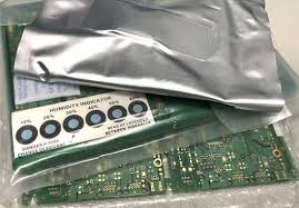
PCBs with ENIG finish can be stored for extended periods (6-12 months) without significant degradation in solderability.
2.4 Suitable for Multiple Reflow Cycles
ENIG can withstand multiple reflow cycles, making it ideal for complex PCB assemblies requiring multiple soldering passes.
2.5 Compatibility with Lead-Free Soldering
Due to RoHS compliance, ENIG is widely used in lead-free soldering processes.
2.6 Good Electrical Conductivity
Gold is an excellent conductor, making ENIG suitable for high-frequency and RF applications.
2.7 Wire Bonding Compatibility
The smooth gold surface allows for reliable gold and aluminum wire bonding, essential in advanced semiconductor packaging.

3. Applications of Immersion Gold PCB Finish
ENIG is widely used in various industries, including:
- Consumer Electronics (Smartphones, Tablets, Laptops)
- Medical Devices (Implantable and diagnostic equipment)
- Automotive Electronics (ECUs, Sensors, Infotainment Systems)
- Aerospace & Defense (High-reliability PCBs)
- Telecommunications (5G, RF, and High-Speed PCBs)
- Industrial Electronics (Control systems, robotics)
4. Manufacturing Process of ENIG Finish
The ENIG process involves several key steps:
Step 1: Cleaning & Microetching
The PCB is cleaned to remove organic contaminants, followed by microetching to roughen the copper surface for better adhesion.
Step 2: Electroless Nickel Deposition
The PCB is immersed in an autocatalytic nickel-phosphorus bath, depositing a uniform nickel layer (3-6 μm).
Step 3: Immersion Gold Deposition
The nickel-coated PCB is dipped into an immersion gold solution, where a displacement reaction deposits a thin gold layer (0.05-0.1 μm).
Step 4: Rinsing & Drying
The PCB is rinsed to remove chemical residues and dried to prevent contamination.
5. Challenges & Potential Issues with ENIG
Despite its advantages, ENIG has some limitations:
5.1 Black Pad Syndrome
A rare but serious defect where excessive phosphorus in the nickel layer leads to weak solder joints and brittle fractures. Proper process control is essential to prevent this.
5.2 Higher Cost
ENIG is more expensive than HASL or OSP due to the use of gold.
5.3 Limited Gold Thickness
The immersion gold layer is very thin, making it susceptible to wear in high-friction applications.
5.4 Not Suitable for High-Power Applications
Nickel has higher resistance than copper, making ENIG less ideal for high-current PCBs.
6. Comparison with Other PCB Surface Finishes
| Finish Type | Advantages | Disadvantages |
|---|---|---|
| ENIG (Immersion Gold) | Flat surface, excellent solderability, long shelf life, RoHS compliant | Higher cost, risk of black pad |
| HASL (Hot Air Solder Leveling) | Low cost, good solderability | Uneven surface, not suitable for fine-pitch components |
| OSP (Organic Solderability Preservative) | Low cost, simple process | Short shelf life, not suitable for multiple reflows |
| Immersion Silver (IAg) | Good solderability, lower cost than ENIG | Prone to tarnishing, shorter shelf life |
| Electrolytic Hard Gold | Extremely durable, excellent wear resistance | Very expensive, requires additional plating steps |
7. Future Trends in PCB Surface Finishes
While ENIG remains popular, new alternatives are emerging:
- ENEPIG (Electroless Nickel Electroless Palladium Immersion Gold) – Adds a palladium layer to improve wire bonding and reduce black pad risk.
- Direct Immersion Gold (DIG) – Eliminates nickel, reducing costs while maintaining performance for certain applications.
- Nanocoating Technologies – Advanced anti-corrosion coatings to extend PCB lifespan.

8. Conclusion
Immersion Gold (ENIG) PCB finish is one of the most reliable and widely used surface treatments in modern electronics. Its excellent solderability, flatness, and compatibility with lead-free processes make it ideal for high-density and high-reliability applications. While it has some drawbacks (such as cost and black pad risk), proper manufacturing controls can mitigate these issues.
As PCB technology evolves, ENIG will continue to be a dominant choice, though alternatives like ENEPIG and DIG may gain traction in specific applications. Engineers and manufacturers must carefully select the right surface finish based on cost, performance, and application requirements.


