The Comprehensive Guide to PCB Leiterplatte: Design, Manufacturing, and Applications
Introduction to PCB Leiterplatte
Printed Circuit Boards (PCBs), known as “Leiterplatte” in German, form the foundational infrastructure of modern electronics. These essential components serve as the physical platform that connects and supports various electronic elements in virtually every electronic device we use today. From smartphones and computers to industrial machinery and medical equipment, PCB Leiterplatte enable the complex interconnection of components that makes modern technology possible.
The term “Leiterplatte” literally translates to “conductor board” in English, perfectly describing the primary function of these components—to provide conductive pathways that allow electrical signals to travel between components. The history of PCB development parallels the evolution of electronics itself, transitioning from simple point-to-point wiring to today’s sophisticated multi-layer designs capable of supporting incredibly complex circuits.
PCB Leiterplatte Materials and Composition
Base Materials
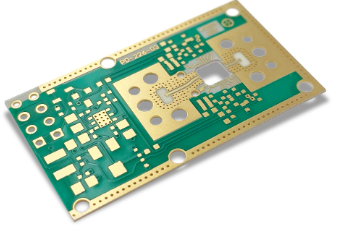
The foundation of every PCB Leiterplatte is its substrate material, typically composed of fiberglass-reinforced epoxy resin known as FR-4. This material offers excellent electrical insulation properties while providing mechanical stability. For high-frequency applications, materials like PTFE (Teflon) or ceramic-filled hydrocarbons may be used to minimize signal loss. Flexible PCBs often employ polyimide films that can withstand repeated bending without failure.
Copper Layers
The conductive pathways on PCBs are created from thin layers of copper foil laminated onto the substrate. Standard PCBs use 1 oz (35 μm) copper, but high-current applications may require 2 oz or thicker copper layers. The copper is typically electrodeposited or rolled onto the substrate, with the manufacturing process influencing the final board’s performance characteristics.
Solder Mask and Silkscreen
A solder mask, usually green (though other colors are available), covers the copper traces to prevent accidental short circuits and protect against environmental factors. The silkscreen layer adds component labels, logos, and other identifying markings using epoxy-based ink. These finishing layers not only protect the board but also aid in assembly and troubleshooting.
Types of PCB Leiterplatte
Single-Sided PCBs
The simplest PCB Leiterplatte design features conductive traces on only one side of the substrate. These cost-effective boards are used in basic electronics where circuit complexity is low, such as in simple power supplies or consumer electronics with limited functionality.
Double-Sided PCBs
With conductive layers on both sides of the substrate, double-sided PCBs offer greater design flexibility. Through-hole vias connect the two layers, allowing more complex circuits in the same physical space. These boards are common in automotive electronics, industrial controls, and more sophisticated consumer devices.
Multi-Layer PCBs
Modern high-density electronics typically use multi-layer PCB Leiterplatte with four, six, eight, or even dozens of conductive layers separated by insulating material. These complex boards enable the miniaturization of advanced electronics by providing multiple routing layers, dedicated power planes, and ground planes that reduce electromagnetic interference.
Flexible and Rigid-Flex PCBs
Flexible PCBs use bendable substrate materials for applications requiring conformity to non-planar surfaces or repeated flexing. Rigid-flex designs combine rigid and flexible sections, offering the benefits of both in applications like foldable electronics or complex three-dimensional packaging.
PCB Leiterplatte Design Process
Schematic Capture
The design process begins with creating a schematic diagram that represents the logical connections between components. Modern electronic design automation (EDA) tools allow engineers to create these schematics digitally, complete with component libraries and design rule checking.
Component Placement
Strategic component placement is crucial for optimal PCB performance. Designers must consider signal flow, thermal management, electromagnetic compatibility, and mechanical constraints when positioning components. High-speed components may need specific placement to minimize signal path lengths, while power components require consideration for heat dissipation.
Routing and Trace Design
The actual conductive pathways are created during routing, where designers or auto-routing software connect components according to the schematic. Critical factors include trace width (determined by current carrying requirements), trace spacing (to prevent crosstalk or short circuits), and impedance control for high-speed signals.
Design Rule Checking (DRC)
Before manufacturing, the design undergoes rigorous DRC to verify compliance with manufacturing capabilities and electrical requirements. This step checks for proper clearances, hole sizes, and other physical constraints to ensure the design can be reliably produced.
PCB Leiterplatte Manufacturing Process
Imaging and Etching
The manufacturing process begins with transferring the circuit pattern onto the copper-clad substrate using photolithography. A photoresist is applied, exposed to UV light through a photomask, and developed to create a protective pattern. The exposed copper is then etched away, leaving only the desired conductive traces.
Layer Alignment and Lamination
For multi-layer boards, individual layers must be precisely aligned before lamination. The layered stack undergoes high pressure and temperature to bond the layers into a single unified board. This critical step ensures proper registration of all layers and vias.
Drilling and Plating
Mechanical or laser drilling creates holes for through-hole components and vias. These holes are then plated with copper to establish electrical connections between layers. Advanced high-density interconnect (HDI) PCBs may use laser-drilled microvias for finer pitch connections.
Surface Finishing
Various surface finishes can be applied to protect exposed copper and ensure solderability. Common finishes include HASL (Hot Air Solder Leveling), ENIG (Electroless Nickel Immersion Gold), and OSP (Organic Solderability Preservative). The choice depends on the application’s requirements for durability, solderability, and cost.
Advanced PCB Leiterplatte Technologies
High-Density Interconnect (HDI)
HDI technology allows for finer traces, smaller vias, and higher connection pad density, enabling more compact and complex designs. This technology is essential for modern smartphones, tablets, and other space-constrained devices.
Embedded Components
Some advanced PCBs embed passive components (resistors, capacitors) within the board layers, saving surface space and improving electrical performance by reducing parasitic inductance. This technology is increasingly important for miniaturized, high-performance electronics.
RF and Microwave PCBs
Specialized PCB Leiterplatte designs cater to high-frequency applications, with careful attention to dielectric materials, impedance control, and signal integrity. These boards are crucial for wireless communications, radar systems, and satellite technology.
Testing and Quality Control
Electrical Testing
Automated optical inspection (AOI) and electrical testing verify proper connectivity and absence of shorts or opens. Flying probe testers or bed-of-nails fixtures check each net on the PCB to ensure it matches the designed connectivity.
Environmental and Reliability Testing
Depending on the application, PCBs may undergo thermal cycling, vibration testing, or humidity exposure to ensure reliability under expected operating conditions. Military and aerospace applications typically require the most rigorous testing protocols.
Applications of PCB Leiterplatte
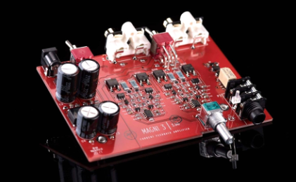
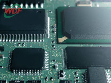
Consumer Electronics
From smartphones to smart home devices, PCBs form the backbone of modern consumer technology. The push for smaller, more powerful devices continues to drive innovation in PCB technology.
Automotive Electronics
Modern vehicles contain dozens of PCBs controlling everything from engine management to infotainment systems. Automotive PCBs must withstand harsh environments including temperature extremes and vibration.
Industrial and Medical Applications
Industrial control systems and medical devices rely on highly reliable PCBs, often with specialized requirements for signal integrity or fail-safe operation. Medical PCBs in particular must meet stringent reliability and sometimes sterilization requirements.
Future Trends in PCB Leiterplatte Technology
Miniaturization and Increased Complexity
The demand for smaller devices with more functionality continues to push PCB technology toward finer features, higher layer counts, and more sophisticated packaging solutions. Advanced packaging techniques like system-in-package (SiP) are blurring the lines between PCBs and integrated circuits.
Sustainable Materials and Processes
Environmental concerns are driving development of lead-free solders, halogen-free substrates, and recycling processes for end-of-life PCBs. The industry is also exploring biodegradable substrates for certain applications.
Integration with Additive Manufacturing
3D printing technologies are beginning to merge with traditional PCB manufacturing, enabling new possibilities for three-dimensional circuit structures and rapid prototyping. This convergence may lead to entirely new approaches to electronic packaging and interconnection.
Conclusion
PCB Leiterplatte technology continues to evolve to meet the demands of an increasingly connected and electronic world. From simple single-layer boards to complex multi-layer HDI designs, these essential components enable the technological advancements that define modern life. As electronics become more pervasive and sophisticated, PCB technology will continue to advance, offering designers new possibilities while facing challenges of miniaturization, signal integrity, and environmental sustainability. Understanding the fundamentals of PCB design and manufacturing remains essential for anyone involved in electronic product development, ensuring that the boards at the heart of our devices meet the rigorous demands of performance, reliability, and efficiency.