PCB Bare Board Manufacturing & Testing Essential Steps
Key Takeaways
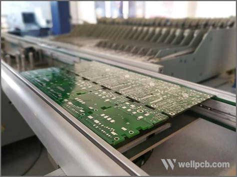
Understanding the essential steps in PCB manufacturing helps you optimize both quality and PCB manufacturing cost. Whether you’re working with PCB manufacturing companies or managing your own PCB manufacturing business, knowing the core processes ensures compliance with design specifications and industry standards.
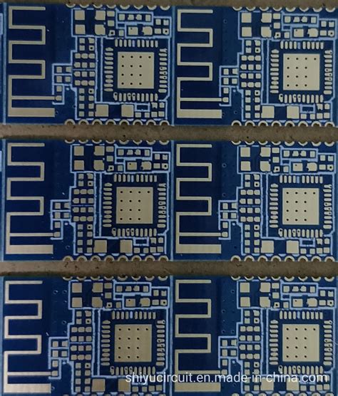
At the foundation lies substrate preparation, where materials like FR-4 are selected for durability and thermal stability. Next, copper layering defines conductive pathways, requiring precise deposition techniques to avoid signal loss. Through-hole drilling follows, with tolerances as tight as ±0.05mm to guarantee component alignment.
| Testing Method | Purpose | Benefit |
|---|---|---|
| Automated Optical Inspection (AOI) | Detects surface defects (e.g., scratches, misalignments) | Reduces human error by 70%+ |
| Electrical Testing | Verifies circuit continuity & isolation | Ensures 99.9% electrical integrity |
Tip: Always request a Design for Manufacturability (DFM) report from your PCB manufacturing partner to preemptively address potential flaws.
Compliance with standards like IPC-6012 ensures reliability, while material choices directly impact performance in extreme environments. For deeper insights into balancing cost and quality, explore this comprehensive guide. By prioritizing these steps, you streamline production timelines and minimize costly rework.
Bare Board PCB Design Fundamentals
When designing a PCB bare board, your choices directly influence manufacturing efficiency, product reliability, and long-term costs. Start by defining your substrate material—common options include FR-4 for general use or high-frequency laminates for specialized applications. The copper layer thickness must align with current requirements, as thicker layers handle higher loads but increase PCB manufacturing cost. Use CAD tools to optimize trace routing, ensuring minimal cross-talk and impedance mismatches.
Collaborating with PCB manufacturing companies early helps identify design constraints, such as minimum drill sizes or spacing tolerances. For instance, through-hole vias smaller than 0.3mm may require advanced drilling techniques, impacting both timelines and budgets. Always validate your design against IPC-2221 standards to avoid rework during PCB manufacturing.
A key consideration is balancing thermal management with layer stack-up. Poor heat dissipation can lead to failures, especially in high-power applications. If you’re running a PCB manufacturing business, integrating design-for-manufacturing (DFM) checks streamlines production and reduces material waste. Remember, even minor oversights in pad sizing or solder mask alignment can escalate costs or delay deliveries. By prioritizing precision in your design phase, you lay the foundation for a robust, compliant board that meets both technical and economic goals.
Copper Layer Deposition Techniques
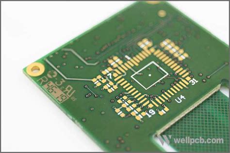
Copper layer deposition forms the conductive foundation of your PCB, directly impacting signal integrity and durability. In PCB manufacturing, two primary methods dominate: electroplating and electroless plating. Electroplating uses an electric current to bond copper ions to the substrate, ensuring precise thickness control—critical for high-frequency applications. Electroless plating, while slower, creates uniform layers without electrical input, ideal for complex geometries.
When selecting a technique, PCB manufacturing companies weigh factors like design complexity and PCB manufacturing cost. Thicker copper layers enhance current capacity but increase material expenses and etching time. Advanced manufacturers often combine both methods, applying electroless plating for initial coverage followed by electroplating to meet specific thickness standards.
Quality hinges on surface preparation. Even minor contaminants can cause voids or delamination, leading to failures during electrical testing. Proper adhesion also relies on surface roughening, which improves mechanical bonding but must balance roughness to avoid impedance issues.
For PCB manufacturing business stakeholders, optimizing deposition processes reduces waste and ensures compliance with industry standards like IPC-6012. By aligning technique choices with design requirements, you maintain performance while managing production timelines and costs effectively.
Through-Hole Drilling Precision Methods
Precision in through-hole drilling defines the reliability of your PCB manufacturing process. Modern PCB manufacturing companies rely on computer-controlled drilling systems to achieve tolerances as tight as ±0.05 mm. These systems use high-speed spindles and carbide drill bits to minimize positional errors, ensuring holes align perfectly with copper layers and design specifications.
To optimize PCB manufacturing cost, operators must balance drill speed, feed rate, and tool longevity. Faster drilling reduces cycle times but risks tool wear, while slower speeds increase accuracy at the expense of production efficiency. Advanced laser drilling methods are increasingly adopted for micro-vias, offering higher precision for high-density designs.
For a successful PCB manufacturing business, maintaining hole wall integrity is critical. Debris removal via vacuum systems and chemical cleaning prevents copper smearing, which can compromise electrical connections. Post-drilling inspections, such as automated optical checks, verify hole placement before moving to plating stages.
By prioritizing precision in drilling, you ensure compliance with industry standards while reducing rework costs—key factors for competitiveness in the PCB manufacturing sector.
Automated Optical Inspection (AOI) Processes
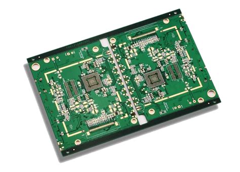
Modern PCB manufacturing relies heavily on Automated Optical Inspection (AOI) to detect defects invisible to the naked eye. During this stage, high-resolution cameras scan the bare board’s surface, comparing captured images against design specifications to identify discrepancies like short circuits, misaligned traces, or missing components. For PCB manufacturing companies, AOI systems reduce human error while ensuring consistency across high-volume production runs—a critical factor in managing PCB manufacturing cost and maintaining profitability.
You’ll find AOI implemented at multiple checkpoints, typically after copper etching and solder mask application. Advanced algorithms analyze layer alignment, pad integrity, and via placement, flagging anomalies for review. This non-contact method preserves board quality without risking physical damage, making it indispensable for PCB manufacturing business models prioritizing precision. By catching flaws early, AOI minimizes rework and prevents defective units from advancing to assembly—saving time and resources.
As compliance standards grow stricter, integrating AOI with machine learning enhances defect classification accuracy. Systems now recognize subtle variations in solder paste coverage or micro-cracks, ensuring boards meet IPC-A-600 guidelines. This synergy between automation and quality control not only streamlines workflows but also reinforces your ability to deliver reliable products in competitive markets. Moving forward, electrical testing builds on AOI results to validate circuit functionality—a seamless progression in the manufacturing chain.
Electrical Testing for Circuit Integrity
After PCB manufacturing companies complete fabrication, verifying circuit integrity becomes critical to ensure your board functions as intended. Electrical testing checks for opens (breaks in conductive paths) and shorts (unintended connections), which can compromise performance or lead to catastrophic failures. Two primary methods are used: flying probe testing for low-volume production and fixture-based testing for high-volume batches.
During testing, automated systems apply voltage to predefined test points, measuring resistance to confirm continuity and isolation. This step directly impacts PCB manufacturing cost, as undetected defects increase scrap rates or rework expenses later. Advanced systems also validate impedance values, ensuring high-speed signal integrity—a must for modern designs like multilayer boards.
While PCB manufacturing prioritizes speed, skipping thorough electrical checks risks long-term reliability. Reputable providers integrate these tests into their PCB manufacturing business workflows to meet industry standards like IPC-6012. For cost-sensitive projects, balancing test coverage with budget requires collaboration between designers and manufacturers to optimize test points without sacrificing quality.
By embedding electrical validation early, you reduce the likelihood of field failures, aligning with compliance goals while safeguarding your product’s reputation.
Bare Board Compliance Standards Overview
When sourcing PCB manufacturing services, understanding compliance standards ensures your bare boards meet industry benchmarks for performance and safety. These standards, such as IPC-6012 for rigid boards or ISO 9001 for quality management, define tolerances for material thickness, copper weight, and hole alignment. PCB manufacturing companies must rigorously follow these guidelines to avoid defects that could escalate PCB manufacturing cost due to rework or delays.
For example, adherence to UL 94 flammability ratings ensures substrates withstand thermal stress, while RoHS directives restrict hazardous substances in materials. During inspections, automated systems verify trace widths and spacing against design files, aligning with IPC-A-600 acceptability criteria. Non-compliance not only risks product failure but can damage the reputation of your PCB manufacturing business, especially in regulated sectors like aerospace or medical devices.
To maintain compliance, prioritize suppliers with certifications like AS9100 or IATF 16949, which validate their processes for precision and traceability. By aligning your requirements with these frameworks, you ensure seamless integration of bare boards into final assemblies while mitigating risks tied to quality deviations.
PCB Substrate Material Selection Guide
Choosing the right substrate material forms the foundation of successful PCB manufacturing. Your selection directly impacts performance, durability, and PCB manufacturing cost, making it critical to balance technical requirements with budget constraints. Common options include FR-4 (flame-retardant epoxy glass), polyimide for high-temperature applications, and ceramic-based substrates for advanced thermal management. Each material offers distinct dielectric properties, thermal conductivity, and mechanical stability—factors that determine compatibility with your design’s electrical and environmental demands.
When working with PCB manufacturing companies, clarify operational parameters like operating temperature ranges, signal frequency, and mechanical stress expectations. For instance, FR-4 suits most consumer electronics due to its cost-effectiveness, while polyimide becomes essential for aerospace or automotive applications requiring extreme heat resistance. Additionally, specialized substrates like Rogers materials minimize signal loss in high-frequency circuits but raise PCB manufacturing business expenses.
Always validate material choices against industry standards (e.g., IPC-4101) to ensure compliance and avoid costly redesigns. By aligning substrate properties with your project’s technical and financial goals, you streamline production and enhance end-product reliability.
Advanced AOI Testing for PCB Quality
When optimizing PCB manufacturing processes, automated optical inspection (AOI) serves as a critical checkpoint for ensuring defect-free boards. Modern AOI systems use high-resolution cameras and machine-learning algorithms to scan bare boards for imperfections like micro-cracks, misalignments, or copper residue—issues that could compromise functionality if undetected. For PCB manufacturing companies, integrating AOI reduces costly rework by identifying errors early, directly impacting PCB manufacturing cost efficiency.
You’ll find AOI applied after etching and drilling stages, where it cross-references design files against physical boards to verify trace accuracy and hole placement. This step is particularly vital for complex multilayer designs, where even minor deviations can cascade into electrical failures. By automating inspections, manufacturers maintain consistency across high-volume production runs—a key advantage in scaling a PCB manufacturing business.
Advanced systems now incorporate 3D imaging to assess solder mask thickness and component pad flatness, further tightening quality control. While AOI can’t replace electrical testing, it complements it by filtering out visual defects before boards proceed to functional validation. For compliance-focused projects, pairing AOI with manual audits ensures adherence to standards like IPC-A-610, safeguarding your reputation in precision-driven industries.
Transitioning to AOI-driven workflows requires balancing upfront investments with long-term savings, but its role in minimizing waste and ensuring reliability makes it indispensable for modern PCB manufacturing operations.
Conclusion
When navigating the complexities of PCB manufacturing, understanding the interplay between design, production, and testing is critical to achieving consistent quality. Whether you’re working with PCB manufacturing companies or managing an in-house PCB manufacturing business, prioritizing precision in steps like substrate preparation and copper layering directly impacts the final product’s reliability. Cost-efficiency remains a key consideration, as PCB manufacturing cost can escalate if processes like through-hole drilling or automated optical inspection (AOI) are not optimized.
By adhering to compliance standards and leveraging advanced testing methods, you ensure that bare boards meet both functional and regulatory requirements. Remember, the choice of substrate materials and electrical testing protocols isn’t just about avoiding defects—it’s about building a foundation for end-product performance. As demands for miniaturization and high-speed circuits grow, refining these processes becomes a strategic advantage in the competitive PCB manufacturing landscape. Ultimately, every decision you make—from material selection to quality assurance—shapes the durability and efficiency of the final assembly.
Frequently Asked Questions
What distinguishes pcb manufacturing for bare boards from assembled PCBs?
Bare board pcb manufacturing focuses solely on creating the substrate, copper layers, and drilled holes without components. Assembled PCBs involve soldering parts onto the bare board, which adds complexity and cost.
How do pcb manufacturing companies ensure quality during production?
Reputable pcb manufacturing companies use automated optical inspection (AOI) and electrical testing to detect defects like short circuits or misaligned drills. These steps validate compliance with design specifications before boards move to assembly.
What factors influence pcb manufacturing cost for bare boards?
Pcb manufacturing cost depends on material choices (e.g., FR-4 vs. high-frequency substrates), layer count, drilling precision, and testing rigor. Bulk orders often reduce per-unit expenses, but tighter tolerances increase upfront costs.
Can small businesses compete in the pcb manufacturing business?
Yes, niche markets like prototyping or low-volume orders allow smaller players in the pcb manufacturing business to thrive. Partnering with agile manufacturers offering flexible MOQs helps balance quality and affordability.
Why is electrical testing critical for bare boards?
Electrical testing confirms circuit continuity and isolation, preventing failures in later stages. Without it, undetected flaws could compromise entire batches, leading to costly rework or recalls.
Ready to Optimize Your PCB Production?
For tailored solutions in pcb manufacturing, please click here to connect with experts who streamline design-to-delivery workflows while adhering to industry standards.