PCB Manufacturing Trends Driving Electronics Innovation
Key Takeaways
The evolution of PCB manufacturing is reshaping how electronics are designed and produced. With HDI technology enabling up to 20-layer boards in smartphones and medical devices, miniaturization is no longer optional—it’s a competitive necessity. PCB manufacturing companies are prioritizing flexible circuits to meet demands for wearables and foldable gadgets, reducing PCB manufacturing cost through automated processes.
"The shift toward high-density designs isn’t just about size—it’s about unlocking performance in 5G and IoT ecosystems," notes a senior engineer at a leading PCB manufacturing business.
| Technology | Impact | Application |
|---|---|---|
| HDI PCBs | 40% thinner traces | 5G base stations, aerospace |
| Flexible Circuits | 30% lighter devices | Wearables, automotive sensors |
| Eco-Friendly Materials | 15% lower carbon footprint | Consumer electronics |
As automotive electrification accelerates, PCB manufacturing adapts with heat-resistant substrates for EV battery systems. Meanwhile, innovations like embedded components are slashing PCB manufacturing cost by integrating functions into fewer layers. For startups, partnering with agile PCB manufacturing companies ensures faster prototyping—critical in a market where every millimeter matters.
Pro Tip: When evaluating PCB manufacturing business partners, prioritize those investing in laser direct imaging (LDI) to minimize defects in high-density designs.
HDI Tech Reshapes PCB Design Standards
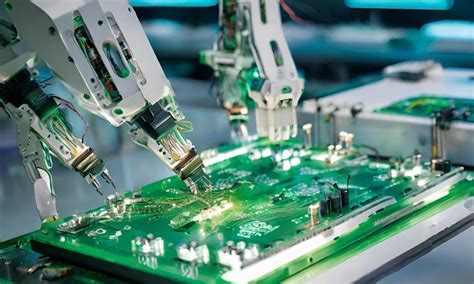
The rise of HDI (High-Density Interconnect) technology is redefining what’s possible in PCB manufacturing, pushing design boundaries to meet demands for smaller, faster, and more reliable electronics. By integrating micro-vias, finer traces, and stacked copper layers, HDI allows PCB manufacturing companies to pack unprecedented functionality into compact spaces—critical for applications like 5G infrastructure and IoT devices. While this innovation elevates performance, it also impacts PCB manufacturing cost, as tighter tolerances require advanced laser drilling and specialized materials.
You’ll notice that adopting HDI forces a reevaluation of traditional design rules. For example, signal integrity in high-speed circuits now demands meticulous impedance matching, while thermal management strategies must account for denser component layouts. Industry leaders are addressing these challenges by deploying AI-driven design tools that optimize layer stacking and via placement, reducing prototyping cycles.
For PCB manufacturing businesses, mastering HDI isn’t optional—it’s a competitive necessity. As consumer expectations shift toward sleeker gadgets, the ability to balance miniaturization with reliability separates leaders from laggards. However, the transition requires upfront investments in equipment and workforce training, reshaping cost structures across the supply chain.
By aligning with HDI standards, designers and manufacturers can future-proof their workflows, ensuring compatibility with next-gen technologies while maintaining scalability. The result? Electronics that aren’t just smaller but smarter, more efficient, and ready to power tomorrow’s innovations.
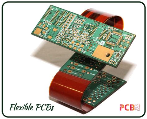
Flexible Circuits Enable Next-Gen Wearables
As devices shrink and demand for seamless integration grows, PCB manufacturing has pivoted toward flexible circuits to power wearable technology. Unlike traditional rigid boards, these ultra-thin, bendable substrates conform to irregular shapes, allowing PCB manufacturing companies to embed electronics into curved surfaces—like smartwatch bands or health-monitoring patches. This shift addresses critical challenges in miniaturization and durability, enabling wearables to withstand daily flexing without compromising performance.
Your fitness tracker’s ability to monitor heart rate or track sleep relies on high-density interconnects (HDIs) within these circuits, which maintain signal integrity even when twisted. Innovations in PCB manufacturing cost reduction—such as roll-to-roll processing—make scalable production feasible, ensuring affordability for mass-market adoption. For startups entering the PCB manufacturing business, partnerships with material scientists are key to optimizing flexible designs without inflating expenses.
These advancements also align with broader industry needs: lighter devices, longer battery life, and enhanced user comfort. As wearables evolve into medical-grade tools, flexible PCBs will underpin breakthroughs like epidermal sensors and AI-driven diagnostics—proving that adaptability isn’t just a feature but a necessity in modern electronics.
5G Systems Demand Advanced PCB Innovations
As you push for faster data transfer and lower latency in 5G systems, the demands on PCB manufacturing intensify. High-frequency signals require substrates with exceptional thermal stability and minimized signal loss, driving PCB manufacturing companies to adopt advanced materials like PTFE or ceramic-filled laminates. These materials not only support millimeter-wave frequencies but also address heat dissipation challenges—critical for densely packed 5G base stations and small-cell deployments.
However, scaling these innovations impacts PCB manufacturing cost. Multilayer designs with ultra-fine traces and microvias add complexity, while stringent quality controls for impedance matching further strain production budgets. For PCB manufacturing business models, balancing performance with affordability becomes a tightrope walk—especially as 5G rollout timelines accelerate globally.
This shift compels engineers to rethink traditional layouts. Embedded components and hybrid rigid-flex designs are gaining traction, enabling compact yet high-performance boards that meet 5G’s rigorous standards. By prioritizing material science breakthroughs and lean manufacturing workflows, the industry can sustainably deliver the precision-driven solutions 5G infrastructure demands.
128B Market Growth Driven by Miniaturization
The relentless push for miniaturization is reshaping how PCB manufacturing companies approach design and production. As devices shrink—from wearables to medical implants—the demand for high-density interconnect (HDI) boards and flexible circuits surges. This trend directly fuels the projected $128 billion market growth by 2030, as smaller, more efficient PCBs become critical for next-gen electronics.
You’ll notice that reducing PCB manufacturing cost while maintaining performance requires innovative techniques like laser drilling and advanced substrate materials. These methods allow tighter trace spacing and higher layer counts, enabling ultra-compact designs without sacrificing reliability. For businesses, this means balancing precision engineering with scalable processes to stay competitive in a market where PCB manufacturing business models increasingly prioritize agility.
Interestingly, the drive for miniaturization isn’t just about size—it’s about enabling smarter functionalities. As 5G and IoT devices demand faster signal transmission, PCB manufacturing must integrate embedded components and multi-functional layers. This evolution challenges traditional workflows but opens opportunities for companies willing to invest in cutting-edge automation and R&D. The result? A market where smaller footprints translate to larger economic impacts.
Smart Devices Thrive on High-Density PCBs
As smart devices shrink in size but grow in capability, PCB manufacturing processes face unprecedented demands. High-density interconnect (HDI) technology enables miniaturization without sacrificing performance, packing more circuitry into thinner, lighter boards. This shift requires PCB manufacturing companies to adopt laser-drilled microvias and stacked copper layers—techniques that refine signal integrity while supporting faster data transfer rates critical for IoT sensors and AI-driven gadgets.
Your smartphone’s 5G connectivity or smartwatch’s health-tracking features rely on these advancements. However, pushing the limits of PCB manufacturing cost structures challenges businesses balancing precision and scalability. Advanced materials like low-loss substrates and embedded components add complexity, but they also reduce failure rates in compact designs. For the PCB manufacturing business, this translates to tighter tolerances and stricter quality controls, driving investments in automation and AI-powered inspection systems.
The ripple effect? Devices become sleeker, smarter, and more energy-efficient—key selling points in competitive consumer markets. Yet, as HDI adoption grows, manufacturers must navigate thermal management hurdles and supply chain dependencies on specialized materials. Those who master this balance will lead the next wave of innovation, where every square millimeter of a PCB unlocks new possibilities for connected ecosystems.

Eco-Friendly Materials Transform PCB Production
As environmental regulations tighten and consumer demand shifts toward sustainability, PCB manufacturing companies are pivoting to eco-friendly materials that reduce ecological footprints without compromising performance. Traditional processes often rely on hazardous chemicals like brominated flame retardants, but innovations such as halogen-free laminates, biodegradable substrates, and lead-free solders are redefining production standards. These materials not only align with global directives like RoHS and REACH but also lower long-term PCB manufacturing cost by minimizing waste disposal fees and regulatory penalties.
Adopting green alternatives also opens new markets for the PCB manufacturing business, particularly in industries prioritizing sustainability, such as electric vehicles and renewable energy systems. For instance, plant-based resins and recyclable copper clads are gaining traction, enabling lighter boards with comparable durability. While transitioning to eco-conscious practices may require upfront investments in R&D, the payoff lies in future-proofing operations against stricter regulations and attracting environmentally aware clients.
By integrating circular economy principles—like reusing scrap metals or recovering rare materials—PCB manufacturing becomes a driver of both innovation and environmental stewardship. This shift isn’t just about compliance; it’s about reimagining how circuits are built to power a cleaner, smarter world.

Automotive Electronics Adopt Flexible PCB Solutions
As vehicles evolve into interconnected hubs of sensors, displays, and autonomous systems, PCB manufacturing must adapt to meet rigorous automotive demands. Flexible circuits are becoming indispensable for modern cars, where space constraints and durability requirements clash with the need for high-speed data transmission. You’ll find vibration-resistant and temperature-tolerant designs in advanced driver-assistance systems (ADAS), infotainment panels, and battery management modules for electric vehicles (EVs).
PCB manufacturing companies are prioritizing lightweight, bendable substrates that conform to irregular shapes while maintaining signal integrity. This shift reduces PCB manufacturing cost by minimizing complex wiring and assembly steps, though material selection—such as polyimide films—remains critical for performance. For automakers, integrating flexible PCBs means faster innovation cycles, as these boards enable seamless upgrades to 5G connectivity and over-the-air software updates.
The PCB manufacturing business is also responding to automotive safety standards, with stricter testing protocols for thermal stability and longevity. By balancing scalability with precision, suppliers ensure flexible circuits meet both miniaturization trends and the ruggedness demanded by next-gen vehicles. As EVs and autonomous driving accelerate, expect flexible PCBs to underpin smarter, safer mobility solutions.
TTM Technologies Leads PCB Manufacturing Evolution
As PCB manufacturing evolves to meet demands for smarter, smaller devices, companies like TTM Technologies are redefining industry benchmarks. By integrating high-density interconnect (HDI) tech and flexible circuit solutions, they’re addressing critical challenges in PCB manufacturing cost and performance scalability. You’ll notice their innovations directly support 5G infrastructure and automotive electronics—sectors requiring ultra-reliable, miniaturized boards. For example, their automated production lines reduce material waste by up to 18%, a game-changer for PCB manufacturing businesses balancing precision and profitability.
What sets TTM apart is their focus on multi-layer flexible PCBs, which enable thinner wearables and faster data transmission in telecom systems. By optimizing laser drilling and advanced lamination processes, they’ve slashed prototyping cycles by 30%, giving PCB manufacturing companies a competitive edge in time-to-market. Their R&D investments also target sustainable materials, aligning with global shifts toward eco-friendly electronics.
As industry demands escalate, TTM’s partnerships with automotive giants and IoT developers highlight how strategic PCB manufacturing adaptations can drive entire ecosystems forward—proving that innovation isn’t just about technology, but reshaping what’s possible.
Conclusion
As you look toward the future of PCB manufacturing, it’s clear that innovation isn’t just reshaping circuit boards—it’s redefining how electronics evolve. PCB manufacturing companies are balancing the demand for miniaturization with the need to reduce PCB manufacturing cost, all while integrating breakthroughs like HDI technology and flexible substrates. These advancements aren’t merely technical upgrades; they’re enabling smaller, smarter devices that power industries from wearables to 5G infrastructure.
For businesses in the PCB manufacturing business, staying competitive means adopting eco-friendly materials and optimizing production workflows. While costs remain a critical factor, the shift toward high-density interconnects and flexible circuits is proving essential to meet the performance demands of modern applications. Automotive systems, for instance, now rely on flexible PCBs to support advanced driver-assistance technologies, illustrating how PCB manufacturing trends directly influence product capabilities.
Ultimately, the trajectory of PCB manufacturing companies hinges on their ability to merge innovation with scalability. By prioritizing R&D and sustainable practices, they can navigate rising complexity without compromising affordability—ensuring the next wave of electronics remains both groundbreaking and accessible.
Frequently Asked Questions
How does miniaturization impact PCB manufacturing costs?
While PCB manufacturing processes for compact designs require advanced equipment, economies of scale in high-volume production often offset initial expenses. Innovations like laser drilling and automated assembly help PCB manufacturing companies balance precision with affordability.
Can flexible circuits reduce long-term business risks?
Yes. Adopting flexible PCBs allows PCB manufacturing businesses to cater to industries like wearables and automotive electronics, which prioritize durability and space efficiency. This diversification mitigates market volatility risks while aligning with 5G and IoT trends.
What drives the $128B market growth forecast for PCBs?
Demand for high-density interconnect (HDI) designs and eco-friendly materials fuels expansion. As devices shrink and performance expectations rise, PCB manufacturing must integrate cutting-edge tech like embedded components and hybrid substrates.
How do eco-friendly practices affect production timelines?
Transitioning to sustainable materials may initially slow workflows, but streamlined recycling processes and energy-efficient machinery improve long-term efficiency. Many PCB manufacturing companies now view sustainability as a competitive advantage.
Explore Advanced PCB Solutions
Ready to optimize your project with next-gen PCB manufacturing? Please click here to discover tailored solutions for high-performance electronics.