Streamlined PCB Assembly and Testing for Compact Electronics
Key Takeaways
Effective PCB assembly and testing in compact electronics demand precision and systematic approaches. Modern PCBA processes leverage surface-mount technology (SMT) and automated pick-and-place systems to ensure accurate component positioning on densely populated boards. To minimize errors, engineers often adopt design-for-manufacturing (DFM) principles, which reduce risks associated with cramped layouts.
"In compact designs, even minor misalignments can cascade into critical failures. Prioritizing PCB assembly validation through pre-production prototyping is non-negotiable."
| Key strategies include: | Technique | Purpose | Tool Example |
|---|---|---|---|
| Automated Optical Inspection (AOI) | Detect soldering defects | 3D AOI scanners | |
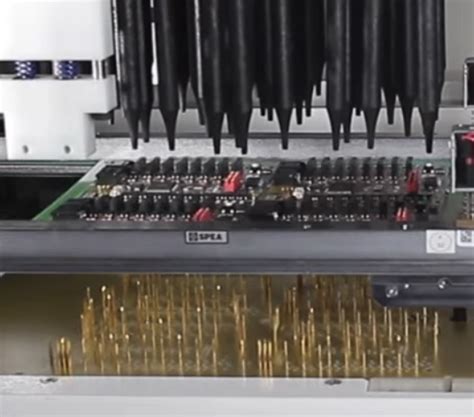
| In-Circuit Testing (ICT) | Validate electrical performance | Bed-of-nails testers | |
| Thermal Profiling | Ensure soldering consistency | Reflow ovens with sensors |
For space-constrained PCBA, micro-via drilling and stacked components optimize real estate usage. Additionally, laser-cut stencils improve solder paste application accuracy, reducing rework.
Pro Tip: Always simulate thermal and mechanical stresses during testing to identify weak points in high-density layouts. Pairing PCB assembly workflows with machine learning-driven analytics further enhances defect detection rates, ensuring reliability in miniature electronics.
By integrating these methods, manufacturers balance efficiency and precision, critical for meeting the demands of modern compact devices.
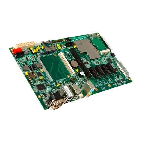
Compact PCB Assembly Techniques
Effective PCB assembly in compact electronics demands meticulous attention to spatial constraints and component density. Modern PCBA processes leverage surface-mount technology (SMT) to accommodate miniature components, ensuring precise placement on tightly spaced boards. Automated pick-and-place systems, paired with vision-guided alignment, reduce human error while handling components as small as 01005 packages. For high-density layouts, stencil printing with ultra-fine-pitch apertures guarantees consistent solder paste application, critical for reliable electrical connections.
Thermal management becomes paramount in compact designs, where heat dissipation challenges escalate. Engineers often integrate high-density interconnect (HDI) substrates and thermally conductive materials to mitigate overheating risks. Additionally, modular assembly workflows—such as panelizing multiple small PCBs—streamline production while maintaining precision. A growing focus on renewable energy solutions has further driven innovations in compact PCB assembly, as seen in applications for solar micro-inverters.
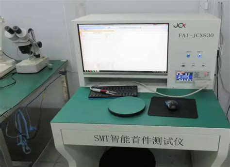
To ensure quality, inline automated optical inspection (AOI) systems verify solder joints and component alignment before proceeding to functional testing. By balancing advanced tools with optimized workflows, manufacturers achieve both scalability and reliability in space-constrained PCBA projects.
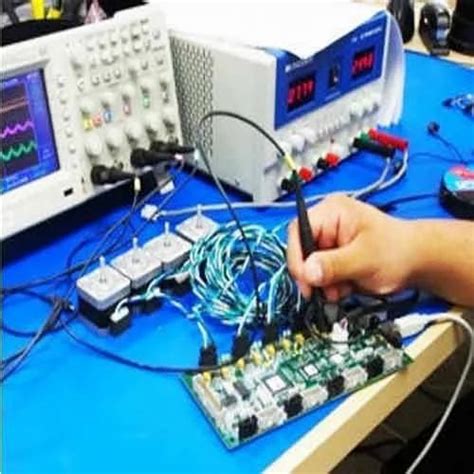
Precision Testing for Miniature Electronics
As electronic components shrink to meet the demands of compact designs, PCB assembly and PCBA processes require meticulous testing protocols to ensure functionality and longevity. Automated optical inspection (AOI) systems, paired with high-resolution imaging, are indispensable for detecting micro-scale solder defects or misalignments in densely packed layouts. For ultra-miniature components, such as 0201 resistors or micro-BGA packages, X-ray inspection provides critical insights into hidden connections, ensuring structural integrity without physical disruption.
Integrating PCBA testing into early design phases reduces rework costs, particularly when validating thermal performance or signal integrity in space-constrained environments. Advanced tools like boundary-scan testing further streamline diagnostics for complex circuits, minimizing downtime. Skilled technicians, such as those profiled in electronics assembly careers, play a vital role in manual verification of sensitive components where automation reaches its limits. By combining automated systems with expert oversight, manufacturers achieve the precision needed to deliver reliable, high-performance miniature electronics.
Minimizing Errors in Compact PCB Assembly
Achieving high accuracy in PCB assembly for space-constrained designs requires meticulous planning and execution. The density of components on compact boards amplifies risks like misalignment, solder bridging, and thermal stress. To mitigate these challenges, manufacturers prioritize automated optical inspection (AOI) systems and precision soldering techniques. For instance, PCBA workflows often incorporate stencil printing with laser-cut apertures to ensure consistent solder paste application, reducing variability in miniature solder joints.
Implementing design for manufacturability (DFM) checks early in the process identifies potential layout conflicts, such as insufficient clearance between high-density ICs or improperly sized pads. Additionally, real-time monitoring during PCB assembly—using tools like thermal profiling and impedance testing—helps detect anomalies before they escalate. Industry experts like Spencer Cave emphasize the value of traceability systems to track component batches, ensuring defective parts are swiftly isolated.
Furthermore, integrating PCBA testing phases—such as in-circuit testing (ICT) and functional validation—into the production line ensures reliability without compromising speed. By balancing automation with rigorous quality protocols, manufacturers can reduce rework rates by up to 40% in compact electronics, aligning with demands for both precision and efficiency.
Optimizing Space-Constrained PCB Workflows
Designing and manufacturing compact electronics demands meticulous planning to balance component density with functional reliability. PCB assembly workflows for space-constrained layouts require specialized approaches, starting with design for manufacturability (DFM) principles. Engineers must prioritize PCBA-compatible component footprints, ensuring adequate clearance for automated pick-and-place systems while avoiding signal interference in tightly packed circuits.
A critical step involves leveraging 3D modeling tools to simulate component placement and routing paths, preempting physical conflicts during PCB assembly. Thermal management strategies, such as strategic via placement or heat-dissipating substrates, become essential in dense layouts to prevent hotspots. Additionally, adopting modular testing protocols early in the workflow—such as in-circuit testing (ICT) or flying probe checks—helps identify faults before final integration, reducing rework cycles.
Collaboration between design and production teams is vital. Standardizing libraries for miniature components (e.g., 0201 resistors or micro-BGAs) streamlines PCBA processes, while automated optical inspection (AOI) systems ensure precision in solder joint quality. By integrating these practices, manufacturers can achieve faster turnaround times without compromising the integrity of compact electronic systems.
Reliable Testing Methods for Dense Layouts
Ensuring reliability in densely packed PCB assembly requires specialized testing protocols to address challenges like signal interference, thermal management, and component accessibility. Automated optical inspection (AOI) systems are critical for detecting soldering defects or misaligned components in PCBA with submillimeter precision, particularly in high-density interconnect (HDI) designs. For boards with hidden connections, X-ray inspection complements AOI by revealing voids in ball grid arrays (BGAs) or microvia integrity.
In-circuit testing (ICT) remains indispensable for validating electrical performance in space-constrained layouts, though fixture design must account for reduced probe accessibility. Transitioning to boundary-scan testing (BST) reduces physical contact points, minimizing risks of damage during validation. Statistical process control (SPC) tools, as highlighted in industry standards, further enhance reliability by analyzing production data to preemptively identify failure trends. Combining these methods ensures robust quality assurance while maintaining alignment with the efficiency goals of compact PCB assembly workflows.
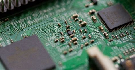
Advanced Tools for Small-Scale Component Assembly
Modern PCB assembly workflows for compact electronics demand specialized tools to address the challenges of miniaturization. High-magnification microscopes and precision pick-and-place machines are indispensable for handling components as small as 01005 packages, ensuring accurate placement without compromising spatial constraints. For PCBA processes, automated optical inspection (AOI) systems equipped with AI-driven defect detection algorithms enhance quality control by identifying soldering flaws or misalignments in densely populated boards.
Advanced reflow soldering ovens with zone-specific temperature control minimize thermal stress on delicate components, while laser soldering tools enable pinpoint accuracy for micro-connections. Engineers also rely on modular assembly jigs tailored to small-form-factor designs, which stabilize boards during manual interventions. Additionally, programmable test fixtures with micro-probes validate electrical continuity in tight layouts, reducing post-assembly troubleshooting.
To streamline workflows, integrated software platforms synchronize design files with assembly machinery, automating component positioning and minimizing human error. These tools not only accelerate production but also ensure consistency across batches—a critical factor for high-reliability applications like medical devices or IoT sensors. By leveraging such technologies, manufacturers achieve repeatable precision in PCB assembly, even when working at sub-millimeter tolerances.
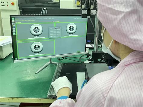
Streamlined Quality Control in Compact Electronics
Implementing effective quality control (QC) in PCB assembly for compact electronics demands specialized strategies to address unique spatial and functional challenges. Automated inspection systems, such as automated optical inspection (AOI) and X-ray imaging, play a critical role in verifying solder joints and component alignment on densely populated PCBA boards. These tools enable rapid detection of microscopic defects—like bridging or cold solder joints—that are common in miniaturized layouts.
To maintain consistency, manufacturers often integrate statistical process control (SPC) methodologies, tracking production metrics in real time to identify deviations early. For example, advanced electromechanical assembly services leverage programmable test fixtures to simulate operational conditions, ensuring components withstand thermal cycling and vibration stresses.
Additionally, modular testing protocols adapt to varying PCB assembly configurations, reducing downtime between batches. By combining inline testing with final functional validation, teams achieve a balance between speed and accuracy—essential for high-mix, low-volume production common in aerospace or medical devices. This multi-layered approach not only minimizes rework but also aligns with lean manufacturing principles, optimizing resource use in space-constrained workflows.
Efficient Component Placement on Small PCBs
Achieving optimal PCB assembly for compact electronics demands meticulous planning to balance spatial constraints with functional requirements. The limited real estate of miniature boards necessitates strategic component orientation and routing prioritization to avoid signal interference or thermal bottlenecks. Engineers often leverage automated pick-and-place systems in PCBA workflows to ensure micron-level accuracy, particularly for surface-mount devices (SMDs) with pitches below 0.4mm. Critical considerations include grouping high-frequency components to minimize trace lengths and isolating heat-generating elements through thermal relief patterns or dedicated copper pours.
To maintain reliability in dense layouts, designers frequently employ multi-layer stacking techniques while adhering to design-for-testability principles. This approach facilitates post-assembly verification, such as in-circuit testing, without requiring physical probe access to every node. Advanced solder paste application methods, including laser-cut stencils, further enhance placement precision for 0402 or smaller packages. As component density increases, real-time optical inspection systems become indispensable for detecting micro-solder bridges or misaligned chips during PCB assembly. By integrating these methodologies, manufacturers can systematically address the unique challenges of space-constrained electronics while maintaining scalable production throughput.
Conclusion
Ultimately, achieving success in PCB assembly and PCBA for compact electronics hinges on harmonizing precision, efficiency, and adaptability. As highlighted throughout this discussion, integrating advanced tools—such as automated pick-and-place systems and high-resolution inspection cameras—ensures accurate component placement even in densely packed layouts. Equally critical are rigorous testing protocols, including automated optical inspection (AOI) and functional testing, which safeguard against defects in space-constrained designs.
To maintain workflow optimization, engineers must prioritize thermal management and signal integrity during both PCB assembly and post-production validation. Leveraging modular testing frameworks, as detailed in resources like specialized tools, can further streamline quality assurance for miniature boards. By adopting iterative design refinements and data-driven error tracking, manufacturers reduce rework cycles while enhancing scalability.
The evolution of PCBA methodologies continues to address challenges posed by miniaturized components and complex interconnects. As compact electronics demand higher performance within shrinking footprints, the fusion of precision assembly techniques and adaptive testing regimes remains indispensable for delivering reliable, high-density solutions.
Frequently Asked Questions
What are the key challenges in assembling components on compact PCBs?
The primary challenges include managing PCB assembly accuracy in limited spaces, avoiding component interference, and ensuring proper heat dissipation. High-density layouts require specialized tools, such as micro-nozzle pick-and-place machines, to maintain precision during PCBA processes.
How can testing reliability be improved for miniature electronics?
Implementing automated optical inspection (AOI) and X-ray testing ensures thorough validation of solder joints and hidden connections in dense PCB assembly. Combining these with in-circuit testing (ICT) helps detect faults early, reducing rework costs and enhancing product durability.
What strategies minimize errors during small-scale PCB production?
Adopting design-for-manufacturing (DFM) principles streamlines PCBA workflows by identifying potential issues in component placement or soldering early. Using laser-cut stencils for solder paste application and adhering to strict ESD protocols further reduces assembly defects.
Can existing workflows be optimized for space-constrained PCB designs?
Yes. Integrating modular fixtures for testing and leveraging software for 3D layout simulations allows engineers to visualize spatial constraints before physical PCB assembly. This approach accelerates prototyping and ensures compatibility with automated assembly lines.
What tools are essential for high-precision compact PCB testing?
Critical tools include flying probe testers for flexible electrical validation, thermal cameras for heat mapping, and boundary scan systems for diagnosing complex ICs. These tools are indispensable for maintaining quality in advanced PCBA projects.
Ready to Optimize Your Compact PCB Assembly Process?
For tailored solutions in PCB assembly and PCBA services designed for compact electronics, please click here to explore expert support and advanced manufacturing capabilities.