The Design and Manufacturing of an 8-Layer PCB Motherboard: A Comprehensive Guide
Introduction to Multilayer PCBs
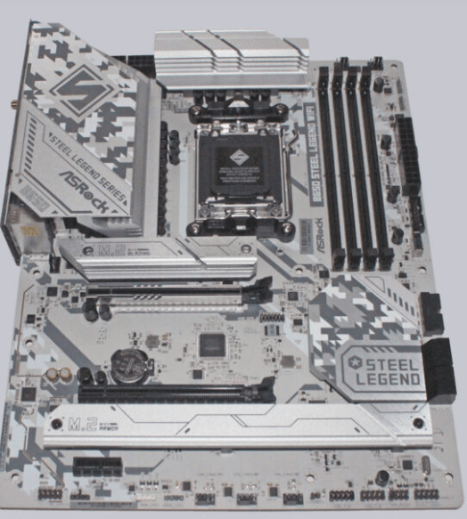
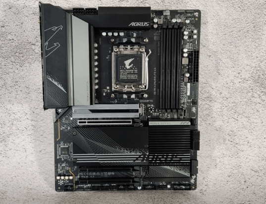
Printed Circuit Boards (PCBs) form the backbone of modern electronics, and as technology advances, the complexity of these boards increases exponentially. Among various configurations, the 8-layer PCB motherboard represents a sophisticated solution that balances complexity with manufacturability, offering significant advantages for high-performance computing systems, networking equipment, and advanced consumer electronics.
An 8-layer PCB stackup provides designers with ample routing channels while maintaining reasonable production costs compared to higher-layer count boards. This makes it particularly suitable for motherboards that need to accommodate high-speed processors, multiple memory channels, various I/O interfaces, and power delivery networks—all within the constrained real estate of standard computer form factors.
Layer Stackup Configuration
The arrangement of layers in an 8-layer PCB is critical to its performance. A typical stackup might include:
- Top Layer (Signal): Primary component placement and high-speed signals
- Ground Plane: Provides return path for top layer signals
- Signal Layer: Inner routing layer
- Power Plane: Primary voltage distribution (e.g., CPU core voltage)
- Power Plane: Secondary voltage distribution (e.g., memory voltage)
- Signal Layer: Inner routing layer
- Ground Plane: Provides return path for bottom layer signals
- Bottom Layer (Signal): Secondary component placement and signals
This symmetrical arrangement helps maintain board stability and minimizes warpage during manufacturing. The adjacent power and ground planes (layers 4 & 5) naturally form a decoupling capacitance that helps with power integrity.
For high-speed designs, alternative stackups might employ more ground planes or specialized prepreg materials to control impedance more precisely. The specific dielectric materials used between layers (typically FR-4 with varying glass weave styles) significantly affect the board’s electrical characteristics.
Design Considerations for 8-Layer Motherboards
Signal Integrity Management
With processor clock speeds exceeding 5 GHz and DDR5 memory interfaces operating at multi-gigabit rates, signal integrity becomes paramount in motherboard design. The 8-layer stackup allows for:
- Controlled impedance routing: Critical for high-speed signals like PCI Express, USB 3.2, and memory buses
- Proper reference planes: Every signal layer should have adjacent ground or power planes
- Differential pair routing: Maintaining consistent spacing and length matching
- Via optimization: Using blind/buried vias or back-drilling to minimize stubs
Power Distribution Network (PDN)
Modern processors can draw over 200 amps at low voltages, making the PDN design crucial:
- Multiple dedicated power planes for core voltages
- Careful via placement to minimize voltage drop
- Proper decoupling capacitor placement
- Plane shapes and splits to accommodate multiple voltage domains
Thermal Management
High-power components require thoughtful thermal design:
- Thermal vias under hot components
- Copper pours connected to ground planes for heat spreading
- Consideration for heatsink mounting
- Potential incorporation of thermal interface materials in the stackup
Manufacturing Tolerances
8-layer boards push standard manufacturing capabilities:
- Typical finished copper weights: 0.5-2 oz
- Minimum trace/space: 3/3 mil (advanced), 4/4 mil (standard)
- Drill sizes: mechanical (≥8 mil), laser (≥4 mil)
- Layer-to-layer registration: ±2 mil
Material Selection
The choice of materials affects performance, cost, and manufacturability:
Standard FR-4: Cost-effective for most applications
High-Tg FR-4: Better thermal performance for lead-free assembly
Low-loss materials: For extreme high-speed designs (e.g., Rogers)
Halogen-free materials: For environmental compliance
The dielectric constant (Dk) and dissipation factor (Df) become increasingly important as signal speeds increase. For DDR5 and PCIe 5.0 interfaces, material selection can make the difference between a working and marginal design.
Routing Strategies
Effective use of all eight layers requires disciplined routing:
- Layer Assignment:
- High-speed signals on top and bottom layers (microstrip)
- Moderate-speed signals on inner layers (stripline)
- Sensitive analog signals with dedicated return paths
- Via Management:
- Minimize via transitions
- Use via-in-pad where necessary
- Consider via shielding for sensitive signals
- Cross-talk Reduction:
- Orthogonal routing on adjacent layers
- Adequate spacing between sensitive signals
- Guard traces for critical nets
- Power Delivery:
- Multiple vias for high-current paths
- Proper plane stitching
- Attention to current return paths
Manufacturing Process
The fabrication of 8-layer PCBs involves numerous precise steps:
- Inner Layer Processing:
- Copper clad laminate preparation
- Photoresist application and imaging
- Etching and stripping
- Automated Optical Inspection (AOI)
- Lamination:
- Layup of cores and prepreg
- Vacuum lamination under heat and pressure
- Controlled cooling to prevent warpage
- Drilling:
- Mechanical drilling of through holes
- Laser drilling for microvias (if used)
- Deburring and cleaning
- Plating:
- Electroless copper deposition
- Electrolytic copper plating
- Optional surface finishes (ENIG, Immersion Silver, etc.)
- Outer Layer Processing:
- Photoresist application and imaging
- Pattern plating and etching
- Solder mask application
- Silkscreen printing
- Final finishing (surface treatment)
- Testing:
- Electrical testing (flying probe or fixture)
- Impedance testing (coupon verification)
- Final inspection
Advanced Technologies in 8-Layer Motherboards
Modern motherboards often incorporate several advanced PCB technologies:
Embedded Components: Passive components buried within the stackup
Via-in-Pad: Plated vias directly in component pads for space savings
Any-layer HDI: Ultra-fine pitch components requiring microvias
Flex-Rigid: Combination of flexible and rigid sections
Heavy Copper: Thicker copper for high-current paths
Challenges in 8-Layer PCB Manufacturing
Producing reliable 8-layer motherboards presents several challenges:
- Registration: Maintaining alignment through multiple lamination cycles
- Interconnect Reliability: Ensuring solid plated through holes
- Material Compatibility: Different materials expanding at different rates
- Warpage Control: Maintaining flatness through thermal cycles
- Yield Management: Each additional layer reduces overall yield
Cost Considerations
While 8-layer boards are more expensive than 4 or 6-layer alternatives, they offer better performance per unit area. Cost factors include:
- Base material costs
- Number of drill hits
- Special requirements (impedance control, tight tolerances)
- Panel utilization efficiency
- Testing requirements
- Lead time considerations
Future Trends
The evolution of 8-layer motherboard technology continues:
- Higher Density Interconnects: Finer lines and spaces
- Advanced Materials: Better thermal and electrical properties
- 3D Integration: Package-on-package technologies
- Embedded Actives: Semiconductor devices within the PCB
- Additive Processes: Semi-additive processing for ultra-fine features
Conclusion
The 8-layer PCB motherboard represents an optimal balance between performance and practicality for many computing applications. Its carefully orchestrated layer stackup provides the necessary resources for power distribution, signal integrity, and component integration that modern systems demand. As processors continue to increase in power and peripherals in number, the 8-layer motherboard will remain a workhorse of computer hardware design, evolving to incorporate new materials and manufacturing techniques to meet ever-growing performance requirements.
Successful design and manufacture of these complex boards requires attention to detail at every stage—from initial material selection and stackup design through careful routing strategies and rigorous manufacturing oversight. By mastering these elements, engineers can produce reliable, high-performance motherboards that form the foundation of today’s advanced electronic systems.