Demystifying Vias in High-Speed PCB Design
Introduction
In high-speed printed circuit board (PCB) design, signal integrity (SI), power integrity (PI), and electromagnetic compatibility (EMC) are critical factors that determine the performance of electronic systems. Among the various elements that influence these factors, vias play a crucial yet often misunderstood role.
Vias are conductive pathways that connect different layers of a PCB, allowing signals and power to traverse between them. While seemingly simple, their impact on high-speed signals can be profound, introducing impedance discontinuities, signal reflections, and crosstalk if not properly designed. This article aims to demystify vias in high-speed PCB design by exploring their types, electrical characteristics, design considerations, and optimization techniques.
1. Types of Vias in PCB Design
Vias come in different forms, each serving specific purposes in PCB layouts:
1.1 Through-Hole Vias
- The most common type, drilled through all layers of the PCB.
- Used for interconnecting signals, power, and ground planes.
- Can introduce significant parasitic inductance and capacitance in high-speed designs.
1.2 Blind Vias
- Connect an outer layer to one or more inner layers but do not go through the entire board.
- Reduce stub effects (unused via portions that cause signal reflections).
- More expensive due to laser drilling requirements.
1.3 Buried Vias
- Exist only between inner layers and are not visible from the outer layers.
- Help in high-density interconnect (HDI) designs.
- Increase fabrication complexity and cost.
1.4 Microvias
- Small-diameter vias (typically < 6 mils) used in HDI designs.
- Can be stacked or staggered to connect multiple layers.
- Essential for high-frequency and high-speed designs due to lower parasitic effects.
2. Electrical Characteristics of Vias
Vias are not ideal conductors; they introduce parasitic elements that affect signal performance:
2.1 Parasitic Inductance
- The via barrel acts as a small inductor, given by:
[
L_{via} \approx \frac{\mu_0 h}{2\pi} \left( \ln \left( \frac{4h}{d} \right) + 1 \right)
]
where: - ( h ) = via length (height)
- ( d ) = via diameter
- Inductive effects cause impedance mismatches and signal ringing, especially in high-speed signals (e.g., PCIe, DDR, USB).
2.2 Parasitic Capacitance
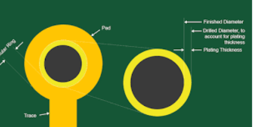
- The via pad and antipad (clearance around the via in planes) form a capacitor:
[
C_{via} \approx \frac{\varepsilon_r \varepsilon_0 \pi D^2}{4h}
]
where: - ( D ) = pad diameter
- ( h ) = dielectric thickness
- Excessive capacitance slows down edge rates and degrades signal quality.
2.3 Impedance Discontinuity
- A via transition creates an impedance mismatch due to its geometry.
- This leads to reflections, particularly in transmission lines (e.g., microstrips, striplines).
2.4 Stub Effects
- In through-hole vias, the unused portion (stub) acts as a resonant structure, causing signal distortion at certain frequencies.
- Blind and buried vias mitigate this issue.
3. Design Considerations for High-Speed Vias
To minimize signal degradation, several design strategies must be employed:
3.1 Via Geometry Optimization
- Diameter: Smaller vias reduce inductance but increase resistance.
- Pad Size: Minimize pad diameter to reduce capacitance.
- Antipad Size: Increase clearance in reference planes to lower capacitance.
3.2 Via Stub Elimination
- Use blind vias or back-drilling (controlled-depth drilling) to remove stubs in through-hole vias.
- Critical for multi-gigabit interfaces (e.g., 10Gbps+ signals).
3.3 Return Path Continuity
- High-speed signals require an uninterrupted return current path.
- Place ground vias adjacent to signal vias to provide a low-inductance return path.
- Avoid splits in reference planes near vias.
3.4 Differential Pair Routing
- Maintain symmetry in via placement for differential pairs to prevent skew.
- Use via shielding (ground vias around signal vias) to reduce crosstalk.
3.5 Via Count Reduction
- Excessive vias increase discontinuities.
- Route critical signals with minimal layer transitions.
4. Advanced Via Techniques in High-Speed Design
4.1 Via-in-Pad
- Places vias directly under component pads to save space.
- Requires filling and plating to prevent solder wicking.
- Common in ball grid array (BGA) designs.
4.2 Tapered Vias
- Gradually change diameter to improve impedance matching.
- Used in RF and millimeter-wave PCBs.
4.3 Via Arrays for Power Delivery
- Multiple vias distribute current and reduce inductance in power delivery networks (PDNs).
- Essential for high-current applications (e.g., processors, FPGAs).
4.4 Simulation and Modeling
- Use 3D electromagnetic (EM) simulators (e.g., HFSS, CST) to analyze via behavior.
- Extract S-parameters to evaluate insertion loss and return loss.
5. Practical Guidelines for Via Design
- For Signals > 1GHz:
- Prefer microvias or blind/buried vias.
- Minimize stub length.
- Maintain consistent impedance.
- For Power Distribution:
- Use multiple vias per power pin.
- Optimize via placement to reduce loop inductance.
- For RF/Microwave Design:
- Implement via fences to suppress surface waves.
- Use grounded coplanar waveguides (GCPW) for controlled impedance.
- For High-Density Designs:
- Leverage HDI techniques with stacked microvias.
- Follow manufacturer capabilities for fabrication.
6. Conclusion
Vias are indispensable in PCB design, but their impact on high-speed signals cannot be overlooked. By understanding their electrical characteristics and applying best practices—such as optimizing geometry, minimizing stubs, ensuring return path continuity, and leveraging advanced techniques—designers can mitigate signal integrity issues and achieve robust high-speed performance.
As data rates continue to rise (e.g., PCIe 6.0, DDR5, 112G SerDes), via design will remain a critical aspect of PCB engineering. Through careful modeling, simulation, and fabrication collaboration, engineers can demystify vias and harness their full potential in next-generation electronic systems.