Multilayer Ceramic PCBs: Design, Manufacturing, and Applications
Abstract
Multilayer ceramic printed circuit boards (PCBs) represent a significant advancement in electronic packaging, offering superior thermal, mechanical, and electrical properties compared to traditional organic PCBs. These boards are widely used in high-frequency, high-power, and high-temperature applications, including aerospace, automotive, medical devices, and telecommunications. This article explores the structure, materials, manufacturing processes, advantages, and key applications of multilayer ceramic PCBs, providing a comprehensive understanding of their role in modern electronics.
1. Introduction
Printed circuit boards (PCBs) are essential components in electronic devices, providing mechanical support and electrical connections between components. While conventional PCBs use organic substrates like FR-4, ceramic PCBs offer enhanced performance in demanding environments. Multilayer ceramic PCBs (MLCCBs) take this a step further by integrating multiple conductive layers within a ceramic substrate, enabling complex circuitry with improved signal integrity, thermal management, and reliability.
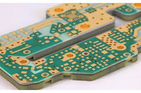
2. Structure of Multilayer Ceramic PCBs
A multilayer ceramic PCB consists of several key components:
- Ceramic Substrate – Typically made from alumina (Al₂O₃), aluminum nitride (AlN), or beryllium oxide (BeO), providing excellent thermal conductivity and electrical insulation.
- Conductive Layers – Usually composed of tungsten (W), molybdenum (Mo), or copper (Cu), forming the circuit traces.
- Via Interconnects – Plated through-holes (PTHs) or laser-drilled microvias that connect different layers.
- Dielectric Layers – Insulating ceramic layers separating conductive traces to prevent short circuits.
- Surface Finishes – Protective coatings such as gold (Au), silver (Ag), or nickel (Ni) to enhance solderability and corrosion resistance.
3. Materials Used in Multilayer Ceramic PCBs
3.1 Ceramic Substrates
- Alumina (Al₂O₃) – The most common choice due to its cost-effectiveness, good mechanical strength, and moderate thermal conductivity (20-30 W/mK).
- Aluminum Nitride (AlN) – Preferred for high-power applications due to its excellent thermal conductivity (140-180 W/mK) and low thermal expansion coefficient.
- Beryllium Oxide (BeO) – Offers the highest thermal conductivity (250-300 W/mK) but is toxic, limiting its use to specialized applications.
3.2 Conductive Materials
- Tungsten (W) and Molybdenum (Mo) – Used in high-temperature co-fired ceramics (HTCC) due to their high melting points.
- Copper (Cu) – Used in low-temperature co-fired ceramics (LTCC) for better conductivity and lower resistance.
3.3 Dielectric Materials
- Glass-ceramic composites are often used in LTCC, while pure ceramics are used in HTCC.
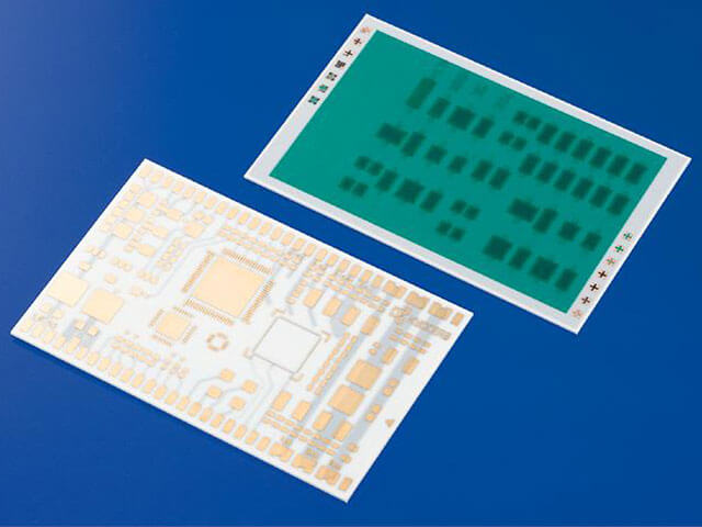
4. Manufacturing Processes
4.1 High-Temperature Co-Fired Ceramic (HTCC)
- Green Tape Casting – Ceramic powder is mixed with organic binders to form flexible sheets.
- Via Formation – Holes are punched or laser-drilled into the sheets.
- Screen Printing – Conductive paste (tungsten/molybdenum) is printed onto the sheets to form circuit patterns.
- Lamination – Multiple layers are stacked and pressed together.
- High-Temperature Firing – The assembly is sintered at 1500-1600°C in a reducing atmosphere.
4.2 Low-Temperature Co-Fired Ceramic (LTCC)
- Green Tape Preparation – Similar to HTCC but with glass-ceramic materials.
- Via Formation and Printing – Conductors (usually silver or gold) are screen-printed.
- Lamination and Firing – Fired at 850-900°C, allowing compatibility with high-conductivity metals like copper.
4.3 Direct Bonded Copper (DBC) and Active Metal Brazing (AMB)
- DBC – Copper foil is bonded to ceramic substrates (AlN/Al₂O₃) at high temperatures.
- AMB – Uses active metals (Ti, Zr) to bond copper to ceramics, improving adhesion.
5. Advantages of Multilayer Ceramic PCBs
- High Thermal Conductivity – Efficient heat dissipation, crucial for power electronics.
- Low CTE (Coefficient of Thermal Expansion) – Matches well with semiconductor materials, reducing thermal stress.
- High-Frequency Performance – Low dielectric loss makes them ideal for RF and microwave applications.
- Chemical and Moisture Resistance – Ceramics are inert, making them suitable for harsh environments.
- Miniaturization – Supports high-density interconnects (HDI) for compact designs.
6. Applications of Multilayer Ceramic PCBs
6.1 Aerospace and Defense
- Used in radar systems, satellite communications, and avionics due to their reliability in extreme conditions.
6.2 Automotive Electronics
- Essential for electric vehicle (EV) power modules, LED lighting, and engine control units (ECUs).
6.3 Medical Devices
- Implantable devices and diagnostic equipment benefit from biocompatibility and high reliability.
6.4 Telecommunications
- 5G infrastructure and RF power amplifiers utilize ceramic PCBs for low signal loss.
6.5 Industrial and Power Electronics
- High-power modules, inverters, and motor drives rely on ceramic substrates for thermal management.
7. Challenges and Future Trends
7.1 Challenges
- High Cost – Ceramic materials and specialized manufacturing increase expenses.
- Fragility – Ceramics are brittle, requiring careful handling.
- Limited Layer Count – Compared to organic PCBs, ceramic PCBs have fewer layers due to processing constraints.
7.2 Future Trends
- Advanced Materials – Development of new ceramic composites with better thermal and electrical properties.
- Additive Manufacturing – 3D printing of ceramic circuits for rapid prototyping.
- Integration with Flexible Electronics – Hybrid designs combining rigid ceramic and flexible substrates.
8. Conclusion
Multilayer ceramic PCBs are a critical technology for high-performance electronics, offering unmatched thermal management, electrical performance, and reliability. While challenges such as cost and brittleness remain, ongoing advancements in materials and manufacturing techniques continue to expand their applications. As industries demand higher power densities and faster signal processing, multilayer ceramic PCBs will play an increasingly vital role in next-generation electronic systems.