Is it okay to have a 90-degree PCB routing angle?
Now, whenever you open the SoC original PCB Layout Guide, you will find that the corner angle of high-speed signal routing will be mentioned. They will say that high-speed signals should not be routed at right angles, but at 45 degrees, and that arcs are better than 45-degree corners.
Is this true? How should the PCB routing angle be set? Is it better to have a 45-degree or arc routing? Is it okay to have a 90-degree right-angle routing?
It has been about the past decade or two since everyone started to worry about the corner angle of PCB routing. In the early 1990s, Intel, the overlord of the PC industry, took the lead in customizing the PCI bus technology.
(Thanks to Intel for releasing the PCI interface. It was the bandwidth improvement of the PCI bus interface, including the later AGP bus interface, that gave birth to graphics cards like 3DFX VOODOO Voodoo. At that time, I also experienced the charm of Tomb Raider Lara for the first time, as well as the exciting Need for Speed 2, the classic Quake, etc. Looking back, it was the market demand for multimedia applications such as 3D games that promoted the development of PC technology, including the later popularity of the Internet and smart phones.)
It seems that starting from the PCI interface, we began to enter an era of “high-speed” system design.
After the 1990s, it was precisely because of a group of such players’ desire for 3D performance that the corresponding electronic design and chip manufacturing technology were able to develop according to Moore’s Law. Due to the continuous improvement of IC process technology, the switching speed of IC transistors is getting faster and faster, and the clock frequency of various buses is getting faster and faster. Signal integrity issues are also constantly attracting everyone’s research and attention. For example, people now have a demand for 4K high-definition home audio and video, and the HDMI2.0 transmission standard rate has reached 18Gbps! ! !
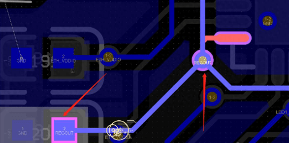
HP3456A has no teardrops, and the right angles are almost intentional (in some places, it should have been completed with an oblique angle, but it insisted on having several consecutive right angles), and there is no copper plating in most places.
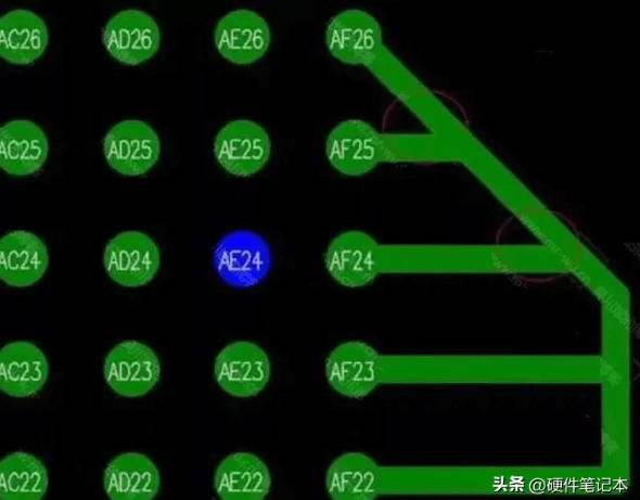
In the upper right corner, not only does it turn right angle, but the line width also becomes smaller?
Right angle, bridge, copper plating, can simulation really not plating copper?
Right angle, 45-degree oblique line, arbitrary angle oblique line, square pad, round pad, but no teardrop.
We will route from acute angle to right angle, obtuse angle, arc to arbitrary angle, and see the advantages and disadvantages of various routing corner angles.
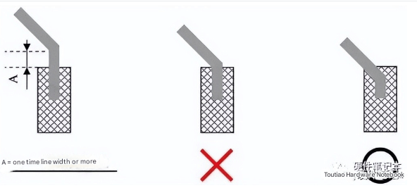
1.Can PCB be routed at sharp angles?
Can PCB be routed at sharp angles? The answer is no. Regardless of whether routing at sharp angles will have a negative impact on high-speed signal transmission lines, from the perspective of PCB DFM, routing at sharp angles should be avoided.
Because at the sharp angles where the PCB wires intersect, there will be a problem called acid traps. What? Sour beans? Well, I like sour beans and noodles, but the acid on the PCB here is a nasty thing. In the PCB board making process, in the PCB line etching link, the “acid traps” will cause excessive corrosion of the PCB line, resulting in the problem of virtual disconnection of the PCB line.
Although we can use CAM 350 to perform DFF Audit to automatically detect the potential problem of “acid traps” to avoid processing bottlenecks when the PCB is manufactured, if the PCB board factory process personnel detect the existence of acid traps, they will simply stick a piece of copper into the gap.
Many engineers in board factories don’t actually understand layout. They just fix the acid trap problem from the perspective of PCB engineering processing, but it is unknown whether this repair will bring further signal integrity problems. Therefore, we should try to avoid acid traps from the source when laying out.
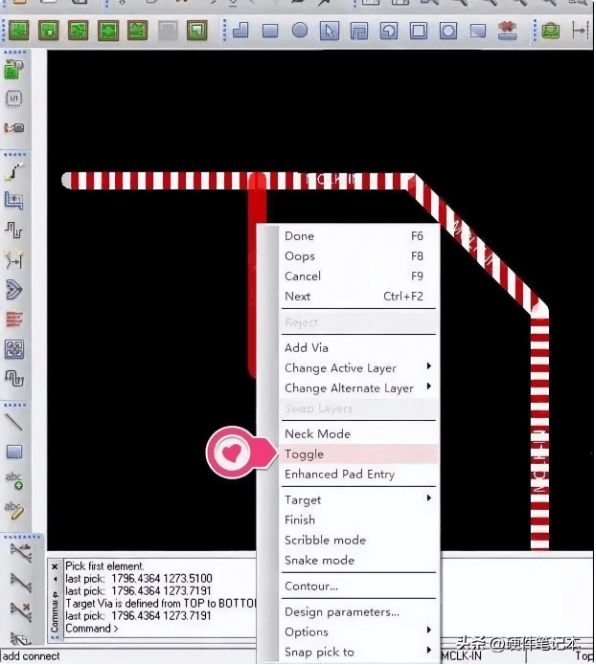
How to avoid sharp angles when pulling wires, causing acid trap DFM problems? Modern EDA design software (such as Cadence Allegro, Altium Designer, etc.) have complete layout routing options. When we are laying out the wiring, we can flexibly use these auxiliary options to greatly avoid the “acid trap” phenomenon when we are laying out.
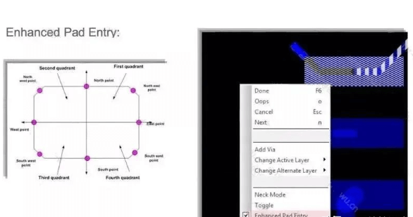
Set the angle of the wire exit of the pad to avoid the angle between the wire and the pad.
Using the Enhanced Pad Entry function of Cadence Allegro allows us to avoid the angle between the wire and the pad when the wire exits as much as possible during layout, avoiding the “acid traps” DFM problem.
Avoid two wires crossing to form a sharp angle.
Flexible application of Cadence Allegro “toggle” option during routing can avoid the formation of sharp angles when the wire is pulled out of the T-shaped branch, avoiding the “acid traps” DFM problem.
2.Can PCB layout be routed at 90°?
High-frequency and high-speed signal transmission lines should avoid routing at 90° corners, which is strongly required in various PCB Design Guides, because high-frequency and high-speed signal transmission lines need to maintain consistent characteristic impedance. When routing at 90° corners, the line width will change at the corners of the transmission line. The line width at the 90° corner is about 1.414 times the normal line width. Since the line width changes, it will cause signal reflection. At the same time, the additional parasitic capacitance at the corner will also cause delays in signal transmission.
Of course, when the signal propagates along the uniform interconnection line, there will be no reflection and distortion of the transmission signal. If there is a 90° corner on the uniform interconnection line, it will cause a change in the PCB transmission line width at the corner. According to relevant electromagnetic theory calculations, this will definitely bring about signal reflection.
This is the case in theory, but theory is theory after all. In actual situations, is the impact of the 90° corner on the high-speed signal transmission line significant?
Therefore, the 90° corner will have a negative impact on high-speed signal transmission lines, which is certain in theory, but is this impact fatal? Does the 90° corner have the same impact on high-speed digital signal and high-frequency microwave signal transmission lines?
According to the paper “right angle corners on printed circuit board traces, time and frequency domain analysis” and Howard Johnson’s article “Who’s Afraid of the Big Bad Bend?” and Eric Bogatin’s book “Signal Integrity and Power Integrity Analysis (Second Edition)” Chapter 8, we can draw the following conclusions:
For high-speed digital signals, the 90° corner will have a certain impact on high-speed signal transmission lines. For our current high-density and high-speed PCBs, the general trace width is 4-5mil, and the capacitance of a 90° corner is about 10fF. According to calculations, the cumulative delay caused by this capacitance is about 0.25ps. Therefore, the 90° corner on a 5mil line width wire will not have a great impact on the current high-speed digital signal (100-psec rise time).
For high-frequency signal transmission lines, in order to avoid signal damage caused by the skin effect, a wider signal transmission line is usually used, such as 50Ω impedance and 100mil line width. The line width at the 90° corner is about 141mil, and the signal delay caused by parasitic capacitance is about 25ps. At this time, the 90° corner will have a very serious impact.
At the same time, microwave transmission lines always hope to reduce signal loss as much as possible. The impedance discontinuity at the 90° corner and the additional parasitic capacitance will cause phase and amplitude errors of high-frequency signals, mismatch between input and output, and possible parasitic coupling, which will lead to deterioration of circuit performance and affect the transmission characteristics of PCB circuit signals.
The impact of a single 90° corner on the signal quality of high-speed digital transmission lines is much greater than the problem caused by the 90° corner, compared with the deviation of the height of the wire and the reference plane, the deviation of the uniformity of the line width and line spacing during the etching process of the wire itself, the change of the dielectric constant of the board on the frequency signal, and even the impact of the parasitic parameters of the via. However, today’s high-speed digital circuit transmission lines always have to be routed with equal lengths. When more than a dozen or twenty corners are superimposed, the signal rise delay caused by the cumulative impact of these 90° corners will become non-negligible. High-speed signals are always transmitted along the impedance path. With 90° corners, the actual signal transmission path will be slightly shorter than the original one.
Moreover, the current high-speed digital signal transmission rate is getting higher and higher. The current HDMI2.0 standard has a transmission bandwidth rate of 18Gbps. 90° corner routing will no longer meet the requirements. Moreover, it is the 21st century now. Even those EDA software that use it now have good support for 45° routing.
At the same time, routing with 90° corners is not in line with people’s aesthetics in terms of engineering aesthetics. Therefore, for the current layout, whether you are routing high-frequency/high-speed signal lines or not, we should try to avoid routing with 90° corners unless there are special requirements.
For high-current routing, we sometimes use copper foil to replace the routing. At the copper corners, we also need to replace the 90° corners with two 45° corners. This is not only beautiful, but also does not pose an EMI risk.
3.Routing at 45 degrees
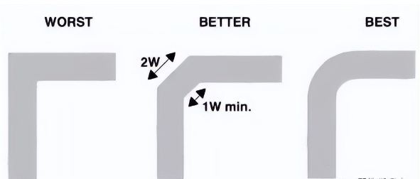
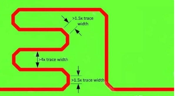
Except for RF signals and other signals with special requirements, the routing on our PCB should preferably be routed at 45 degrees. One thing to note is that when the 45° angle routing is equal in length, the routing length at the corner should be at least 1.5 times the line width, and the spacing between the equal-length lines should be at least 4 times the line width.
Since high-speed signal lines are always transmitted along the impedance path, if the spacing between the equal-length lines is too close, due to the parasitic capacitance between the lines, the high-speed signal takes a shortcut, and the equal length will be inaccurate. The winding rules of modern EDA software can easily set the relevant winding rules.
4.Arc routing
If the technical specifications do not explicitly require arc routing, or if it is an RF microwave transmission line, I personally think that there is no need to use arc routing, because the layout of high-speed and high-density PCBs, a large number of arcs are very troublesome to repair later, and a large number of arc routing also takes up more space.
Of course, for RF microwave signal transmission lines, it is still preferred to use arc routing, or even “45° external bevel” routing.
5 Routing at any angle
With the development of 4G/5G wireless communication technology and the continuous upgrading of electronic products, the current PCB data interface transmission rate has reached 10Gbps or above 25Gbps, and the signal transmission rate is still developing towards high speed. (Thanks for following the official account: Hardware Notebook) With the development of high-speed and high-frequency signal transmission, higher requirements are placed on PCB impedance control and signal integrity.
For digital signals transmitted on PCB boards, many dielectric materials including FR4 used in the electronics industry have always been considered uniform when transmitted at low speed and low frequency.
However, when the electronic signal rate on the system bus reaches the Gbps level, this uniformity assumption no longer holds. At this time, the local changes in the relative dielectric constant of the dielectric layer caused by the gaps between the glass fiber bundles interwoven in the epoxy resin substrate will not be ignored. The local disturbance of the dielectric constant will make the delay and characteristic impedance of the line related to space, thereby affecting the transmission of high-speed signals.
Test data based on FR4 test substrates show that due to the relative position difference between the microstrip line and the glass fiber bundle, the measured effective dielectric constant of the transmission line fluctuates greatly, and the difference in the value can reach △εr=0.4. Although these spatial perturbations seem small, they will seriously affect differential transmission lines with data speeds of 5-10Gbps.
In some high-speed design projects, in order to cope with the impact of the glass fiber effect on high-speed signals, we can use zig-zag routing technology to mitigate the impact of the glass fiber effect.
Cadence Allegro PCB Editor 16.6-2015 and subsequent versions bring support for zig-zag routing mode.
In the Cadence Allegro PCB Editor 16.6-2015 menu, select “Route -> Unsupported Prototype -> Fiber Weave Effect” to turn on the zig-zag routing function.
Therefore, there is no unchanging PCB layout rule. With the improvement of PCB manufacturing technology and the increase of data transmission rate, it is possible that the correct rules now will no longer apply in the future.