EMC Considerations in PCB Design: A Comprehensive Guide
1. Introduction
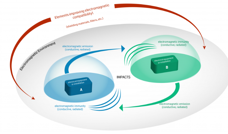
Electromagnetic Compatibility (EMC) is a critical aspect of printed circuit board (PCB) design that ensures electronic devices operate as intended without causing or suffering from electromagnetic interference (EMI). Poor EMC design can lead to signal integrity issues, radiated emissions, susceptibility to external noise, and even regulatory compliance failures.
This article explores key EMC considerations in PCB design, including grounding strategies, signal integrity, component placement, routing techniques, and shielding methods. By implementing these best practices, engineers can minimize EMI and enhance the reliability of electronic systems.
2. Understanding EMC and EMI
2.1 Electromagnetic Compatibility (EMC)
EMC refers to a device’s ability to:
- Emit minimal electromagnetic interference (EMI) that could affect other devices.
- Resist external EMI from other sources without malfunctioning.
2.2 Electromagnetic Interference (EMI)
EMI can be categorized as:
- Conducted EMI – Noise transmitted through power or signal lines.
- Radiated EMI – Noise emitted as electromagnetic waves.
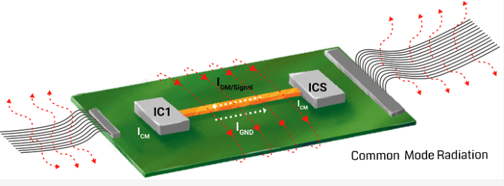
Common sources of EMI in PCBs include:
- High-speed digital signals
- Switching power supplies
- Clock oscillators
- Poor grounding and return paths
3. Key EMC Considerations in PCB Design
3.1 Proper Grounding Techniques
Grounding is crucial for minimizing noise and ensuring signal integrity.
3.1.1 Single-Point vs. Multi-Point Grounding
- Single-point grounding is ideal for low-frequency circuits to avoid ground loops.
- Multi-point grounding is better for high-frequency circuits to reduce impedance.
3.1.2 Ground Plane Design
- Use a solid ground plane to provide a low-impedance return path.
- Avoid split ground planes unless necessary (e.g., analog/digital separation).
- Ensure stitching vias connect ground layers in multilayer PCBs.
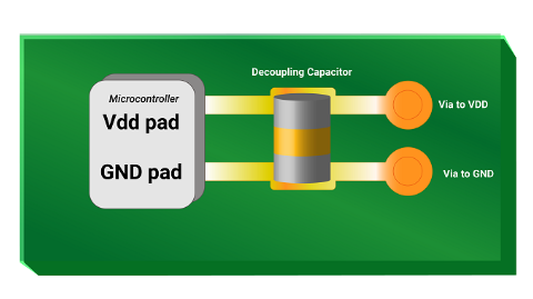
3.2 Power Distribution Network (PDN) Design
A well-designed PDN reduces noise and voltage fluctuations.
- Use decoupling capacitors near IC power pins to filter high-frequency noise.
- Implement power planes to minimize loop inductance.
- Separate analog and digital power supplies to prevent coupling.
3.3 Signal Integrity and Controlled Impedance
High-speed signals require careful routing to prevent reflections and crosstalk.
- Match trace impedance to the source and load (e.g., 50Ω for RF signals).
- Minimize sharp bends (use 45° or curved traces instead of 90° turns).
- Route differential pairs closely to maintain symmetry and reduce EMI.
3.4 Component Placement for EMC
Strategic component placement reduces EMI and improves performance.
- Keep high-speed components (clocks, processors) away from sensitive analog circuits.
- Place decoupling capacitors as close as possible to power pins.
- Group related components (e.g., power supply section, RF section).
3.5 PCB Layer Stackup Optimization
A well-designed layer stackup minimizes EMI and improves signal integrity.
- 4-Layer PCB Example:
- Top Layer: Signal traces (high-speed signals)
- Ground Plane
- Power Plane
- Bottom Layer: Low-frequency signals and routing
- 6-Layer PCB Example:
- Top Layer: High-speed signals
- Ground Plane
- Signal Layer
- Power Plane
- Signal Layer
- Bottom Layer: Low-speed signals
3.6 Shielding and Filtering Techniques
When EMI cannot be eliminated through layout, shielding and filtering are necessary.
- Use shielded enclosures for sensitive circuits.
- Implement ferrite beads and EMI filters on power and signal lines.
- Apply conductive coatings (e.g., copper tape) for additional shielding.
3.7 Clock and High-Speed Signal Routing
Clock signals are major EMI sources and require special attention.
- Keep clock traces short and direct.
- Use guard traces or ground shielding around clock lines.
- Avoid routing clocks near sensitive analog signals.
3.8 Minimizing Loop Areas
Large current loops act as antennas, radiating EMI.
- Route signal traces close to their return paths.
- Use ground planes beneath high-frequency traces.
- Avoid splitting return paths with slots or gaps.
4. Common EMC Design Mistakes to Avoid
- Ignoring return current paths – Leads to ground loops and increased EMI.
- Poor decoupling capacitor placement – Reduces effectiveness in filtering noise.
- Long, unshielded high-speed traces – Increases radiated emissions.
- Inadequate power plane design – Causes voltage drops and noise.
- Mixing analog and digital grounds improperly – Introduces noise coupling.
5. Testing and Compliance
5.1 Pre-Compliance Testing
Before formal certification, conduct in-house tests:
- Near-field probes to detect EMI hotspots.
- Spectrum analyzers to measure radiated emissions.
- Conducted emission tests using LISNs (Line Impedance Stabilization Networks).
5.2 Regulatory Standards
Common EMC standards include:
- FCC Part 15 (USA) – Regulates unintentional radiators.
- CISPR 22/32 (International) – Limits EMI for IT equipment.
- EN 55032 (EU) – EMC requirements for multimedia devices.
6. Conclusion
Designing PCBs with EMC in mind is essential for ensuring reliable operation and regulatory compliance. By implementing proper grounding, power distribution, signal routing, and shielding techniques, engineers can significantly reduce EMI and improve system performance.
Key takeaways:
- Use solid ground planes and minimize loop areas.
- Optimize layer stackup for signal integrity.
- Route high-speed signals carefully and shield sensitive circuits.
- Test early and often to identify EMI issues before certification.
By following these best practices, PCB designers can create robust, high-performance electronic systems that meet stringent EMC requirements.