Factors Affecting Signal Loss in Printed Circuit Boards (PCBs)
Introduction
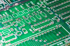
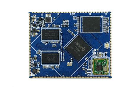
Printed Circuit Boards (PCBs) form the backbone of modern electronics, providing both mechanical support and electrical connections between components. As electronic devices continue to push towards higher frequencies and faster data rates, understanding and controlling signal loss in PCBs has become increasingly critical. Signal loss in PCBs can degrade system performance, limit maximum operating frequencies, and reduce signal integrity. This article examines the key factors that contribute to loss in PCBs, including dielectric materials, conductor properties, design considerations, environmental factors, and manufacturing variations.
1. Dielectric Material Properties
The substrate material between PCB conductors plays a fundamental role in determining signal loss characteristics. Several dielectric properties significantly impact overall loss:
1.1 Dielectric Constant (Dk)
The dielectric constant, or relative permittivity (εᵣ), affects both the speed of signal propagation and the impedance characteristics of transmission lines. While Dk doesn’t directly cause loss, its frequency-dependent behavior contributes to loss mechanisms:
- Higher Dk materials generally show greater dispersion (variation with frequency)
- Dk stability across frequency is crucial for maintaining consistent impedance
- Typical FR-4 has Dk around 4.3-4.8 at 1 GHz, while high-frequency materials may range from 2.2-3.5
1.2 Dissipation Factor (Df)
The dissipation factor (loss tangent) represents the dielectric’s inherent energy absorption:
- Df quantifies the ratio of energy lost to energy stored in the dielectric material
- Common FR-4 has Df of 0.015-0.025, while high-performance materials may be <0.002
- Dielectric losses increase linearly with frequency (α_d ∝ f × Df × √εᵣ)
1.3 Frequency Dependence
Dielectric properties typically vary with frequency:
- Most materials show decreasing Dk and increasing Df with frequency
- Resonance effects in dielectric materials can cause abrupt changes in loss characteristics
- Material selection must consider the operating frequency range
1.4 Common PCB Dielectric Materials
| Material | Dk (1 GHz) | Df (1 GHz) | Typical Applications |
|---|---|---|---|
| Standard FR-4 | 4.3-4.8 | 0.015-0.025 | Consumer electronics, low-speed digital |
| High-Tg FR-4 | 4.0-4.5 | 0.010-0.020 | Industrial, automotive, moderate frequency |
| Rogers RO4003C | 3.38 | 0.0027 | RF/microwave, high-speed digital |
| Isola I-Tera | 3.45 | 0.0031 | High-speed networking, 5G |
| PTFE (Teflon) | 2.1 | 0.0004 | Millimeter-wave, aerospace |
2. Conductor Loss Mechanisms
The metal traces in PCBs contribute significantly to overall loss, particularly at higher frequencies where skin effect dominates:
2.1 Skin Effect
As frequency increases, current crowds toward the conductor surface:
- Skin depth (δ) = √(ρ/πfμ), where ρ is resistivity, f is frequency, μ is permeability
- At 1 GHz, skin depth in copper is about 2.1 μm
- Effective resistance increases as R ∝ √f due to reduced conduction area
2.2 Surface Roughness
Copper foil roughness increases conductor loss:
- Rough surfaces increase effective conductor length and resistance
- Can increase loss by 20-50% compared to smooth conductors at high frequencies
- Typical treatments: STD (standard), RTF (reverse treat), HVLP (very low profile)
2.3 Copper Quality and Thickness
- Impurities in copper increase resistivity
- Thinner traces have higher resistance (but thinner dielectrics allow narrower traces)
- 1 oz (35 μm) copper common, high-current designs may use 2 oz or thicker
2.4 Oxidation and Surface Treatment
- Copper oxidation increases surface resistance
- Surface finishes (ENIG, immersion silver, OSP) affect loss differently
- ENIG (Electroless Nickel Immersion Gold) can introduce additional loss due to nickel layer

3. Design Factors Affecting PCB Loss
Beyond material selection, numerous design decisions impact signal loss:
3.1 Transmission Line Geometry
The type and dimensions of transmission lines significantly affect loss:
Microstrip (surface trace over ground plane):
- Most common for outer layers
- Loss typically lower than stripline for same dielectric
- Susceptible to environmental effects
Stripline (embedded between two ground planes):
- Lower radiation loss than microstrip
- Generally higher dielectric loss due to longer path in dielectric
- Better isolation between signals
Coplanar Waveguide:
- Offers good high-frequency performance
- Requires careful ground plane management
- Lower dispersion than microstrip
3.2 Impedance Control and Matching
- Mismatched impedance causes reflections that effectively increase loss
- Tolerances in fabrication affect achievable impedance control
- Typical high-speed designs aim for ±10% impedance tolerance
3.3 Via Structures
Vias necessary for multilayer boards introduce discontinuities:
- Stub effects (unused via portions) cause resonances and reflections
- Via diameter, pad size, and antipad clearance affect capacitance
- Backdrilling can remove stubs but adds cost
- Microvias help reduce parasitic effects in HDI designs
3.4 Routing Considerations
- Curves and corners should use gradual bends (45° or curved)
- Acute angles can cause reflections and increased loss
- Differential pairs require careful length matching
- Crosstalk from adjacent signals effectively increases loss

4. Environmental Factors
Operating conditions can alter PCB loss characteristics:
4.1 Temperature Effects
- Dielectric Dk and Df typically increase with temperature
- Copper resistance increases with temperature (α ≈ 0.0039/°C)
- High Tg materials maintain properties better at elevated temperatures
4.2 Humidity Absorption
- Most dielectric materials absorb moisture, increasing Df
- Hydrophobic materials like PTFE less affected
- Baking can remove absorbed moisture
4.3 Mechanical Stress
- Flexing can alter transmission line geometry
- Delamination changes dielectric properties
- Conductor cracking increases resistance

5. Manufacturing Variations
Fabrication processes introduce variability that affects loss:
5.1 Dielectric Thickness Control
- Typical ±10% thickness variation affects impedance and loss
- Thinner dielectrics increase conductor loss dominance
- Thicker dielectrics increase dielectric loss portion
5.2 Copper Etching Quality
- Over-etching reduces trace width, increasing resistance
- Under-etching leaves residual copper, affecting impedance
- Etch factor (sidewall angle) affects high-frequency current distribution
5.3 Layer-to-Layer Registration
- Misalignment between layers affects impedance consistency
- Particularly important for stripline designs
- HDI designs with microvias require tight registration
5.4 Surface Finish Quality
- Rough or uneven finishes increase conductor loss
- Thickness variations in plating affect high-frequency performance
- Intermetallic compounds in some finishes may increase loss
6. Measurement and Characterization
Accurate loss measurement is essential for validation:
6.1 Test Methods
- Time Domain Reflectometry (TDR) for impedance verification
- Vector Network Analysis (VNA) for S-parameter measurement
- Resonant methods for dielectric property extraction
6.2 Calibration Considerations
- Proper calibration standards required
- De-embedding techniques to isolate DUT effects
- Fixture design critical for accurate measurements
6.3 Correlation with Simulation
- EM simulation tools help predict loss during design
- Measurement validation improves model accuracy
- Material characterization needed for reliable simulation
Conclusion
PCB signal loss results from complex interactions between materials, design choices, manufacturing processes, and operating conditions. At lower frequencies, conductor resistance dominates, while dielectric losses become increasingly important as frequencies rise into the GHz range. Modern high-speed designs require careful consideration of all loss mechanisms, often necessitating trade-offs between performance, cost, and manufacturability. By understanding these factors, engineers can select appropriate materials, optimize designs, and specify fabrication requirements to achieve the necessary signal integrity for their applications. Future developments in low-loss materials, improved manufacturing techniques, and advanced design methodologies will continue to push the boundaries of PCB performance.
