Precision Techniques in Surface Mount PCB Assembly Optimization

Key Takeaways
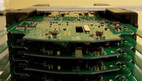
Effective PCB assembly processes rely on precision-driven strategies that balance speed with accuracy. Modern PCBA workflows integrate automated optical inspection (AOI) and statistical process control (SPC) to minimize defects while maintaining throughput. Critical considerations include optimizing solder paste deposition for fine-pitch components and ensuring thermal profiles align with material specifications. Advanced pick-and-place systems enhance component alignment accuracy, directly impacting yield rates in high-volume production. For cost efficiency, manufacturers increasingly adopt closed-loop feedback systems to refine process parameters in real time. Key metrics such as first-pass yield (FPY) and mean time between failures (MTBF) remain central to evaluating assembly line performance. By prioritizing traceability protocols and environmental stress testing, PCB assembly teams can mitigate risks in mission-critical applications. These foundational practices not only streamline PCBA workflows but also ensure compliance with industry standards like IPC-A-610 and J-STD-001, laying the groundwork for deeper exploration of automated placement and soldering methodologies in subsequent sections.

Automated SMT Placement Strategies
Modern PCB assembly processes rely heavily on automated surface mount technology (SMT) placement systems to achieve the speed and precision required for high-volume production. Advanced pick-and-place machines equipped with vision-guided robotics enable micron-level accuracy when positioning components, minimizing errors caused by manual handling. These systems leverage CAD data and real-time feedback mechanisms to optimize component orientation and placement sequence, reducing cycle times by up to 40% compared to semi-automated workflows.
A critical factor in optimizing PCBA efficiency lies in balancing placement speed with thermal management. High-speed machines often integrate nozzle-switching technology to handle diverse component sizes without interrupting production, while intelligent software dynamically adjusts placement pressure to prevent damage to delicate parts. For industries requiring traceability, automated SMT lines incorporate RFID tagging and barcode scanning to track components from feeder to board, ensuring compliance with stringent quality standards.
To further enhance reliability, manufacturers are adopting closed-loop calibration systems that automatically compensate for mechanical drift during extended operations. This approach, combined with predictive maintenance algorithms, reduces downtime by 25–30% in high-mix environments. For insights into scalable solutions, industry leaders like Fineline Global Group emphasize the importance of modular SMT platforms that adapt to evolving design complexities. As assembly lines transition toward Industry 4.0, seamless integration between placement machinery and downstream processes—such as reflow soldering—becomes pivotal for maintaining throughput and consistency.
Precision Soldering for Reliable PCBs
Precision soldering forms the backbone of high-quality PCB assembly, ensuring electrical continuity and mechanical stability in PCBA manufacturing. Modern techniques leverage laser-assisted soldering and nitrogen-reflow environments to minimize oxidation and achieve consistent joint formation. For instance, reflow soldering with optimized thermal profiles ensures uniform heat distribution across components, reducing defects like tombstoning or cold joints.
| Soldering Method | Key Advantage | Typical Application |
|---|---|---|
| Vapor Phase | Low thermal stress | Sensitive components |
| Selective Soldering | Targeted precision | Mixed-technology boards |
| Laser Soldering | Micron-level accuracy | High-density interconnects |
Advanced PCBA processes integrate real-time monitoring systems to track solder paste deposition and joint quality. Automated optical inspection (AOI) paired with X-ray verification detects micro-cracks or voids invisible to the naked eye. Manufacturers adopting closed-loop feedback systems can dynamically adjust soldering parameters, enhancing yield rates by up to 15%.
Critical to success is the interplay between solder alloy composition and flux chemistry. Lead-free SAC305 alloys, for example, require precise temperature control to maintain wettability without damaging temperature-sensitive ICs. By aligning material science with process engineering, PCB assembly achieves reliability standards exceeding IPC-A-610 Class 3 for mission-critical applications.
Quality Control in SMT Assembly Lines
Effective PCB assembly processes rely on rigorous quality control systems to mitigate defects and ensure consistent performance in PCBA production. Modern surface mount technology (SMT) lines employ multi-stage inspection protocols, beginning with automated optical inspection (AOI) systems that scan solder paste deposition and component placement accuracy at micron-level resolutions. These systems flag deviations such as tombstoning or misaligned ICs before reflow soldering, reducing rework costs by up to 40%. Post-soldering, X-ray inspection validates hidden connections like ball grid arrays (BGAs), while functional testing simulates real-world operating conditions to identify latent failures.
Advanced statistical process control (SPC) tools analyze production data in real time, correlating variables like temperature profiles and conveyor speeds to defect rates. This enables manufacturers to fine-tune parameters dynamically, maintaining PCB assembly yields above 99.5% in high-volume environments. Environmental controls further enhance reliability, with humidity-regulated workspaces preventing oxidation of sensitive components during PCBA handling. By integrating machine learning algorithms, quality systems predict equipment wear patterns, scheduling preventive maintenance before precision tolerances degrade. Such proactive measures not only align with ISO 9001 standards but also create seamless transitions into downstream optimization phases, such as automated process adjustments based on historical performance data.
Optimizing SMT Assembly Automation
Modern PCB assembly workflows achieve peak efficiency through advanced automation systems that integrate component placement, soldering, and inspection processes. Automated pick-and-place machines equipped with vision-guided systems ensure micron-level accuracy when positioning surface-mount devices (SMDs), reducing placement errors by up to 98% compared to manual methods. For PCBA lines, optimizing conveyor synchronization between stencil printers, reflow ovens, and inspection stations minimizes bottlenecks while maintaining thermal consistency during soldering.
Tip: Implement machine learning algorithms to predict maintenance needs for robotic arms, cutting unplanned downtime by 30–40% in high-volume production environments.
Real-time feedback loops using automated optical inspection (AOI) enable immediate correction of solder defects or misalignments, ensuring compliance with IPC-A-610 standards. To further streamline SMT assembly automation, manufacturers are adopting modular systems that allow rapid reconfiguration for mixed-product batches. For instance, dual-lane conveyors paired with high-speed chip shooters can process 80,000 components per hour without compromising placement precision.
Balancing speed and accuracy requires precise calibration of nozzle pressure, vacuum strength, and feeder alignment in pick-and-place units. Advanced PCBA facilities now utilize digital twins to simulate production runs, identifying potential bottlenecks before physical assembly begins. This approach not only optimizes cycle times but also reduces material waste by validating component layouts in virtual environments.
Cost-Effective SMT Assembly Methods
Achieving cost efficiency in PCB assembly requires balancing advanced technologies with strategic process design. A foundational step involves optimizing automated component placement systems to minimize material waste and cycle times. By implementing PCBA-specific software for real-time feeder optimization, manufacturers can reduce setup changes by up to 30%, directly lowering labor and machine downtime costs.
Material selection plays a pivotal role—using standardized solder paste formulations with extended shelf lives cuts replenishment expenses, while precision stencil designs ensure consistent deposition rates, reducing rework. Integrating lean manufacturing principles into SMT assembly lines further enhances cost-effectiveness by streamlining workflows and minimizing contamination risks in critical stages like reflow soldering.
For high-volume production, panelization strategies that maximize board space utilization can decrease per-unit costs by 15–20%. Pairing this with modular PCB assembly equipment allows scalable upgrades without full-line overhauls. Finally, predictive maintenance protocols for pick-and-place machines and reflow ovens prevent unplanned stoppages, ensuring sustained throughput. This approach not only aligns with broader quality control frameworks but also reinforces the economic viability of modern PCBA manufacturing.
SMT Process Optimization Techniques
Effective PCB assembly relies on refining SMT workflows to balance speed, accuracy, and cost-efficiency. Central to this is optimizing pick-and-place systems through advanced vision alignment and nozzle configurations, which reduce placement errors by up to 30% in high-density PCBA designs. Implementing dynamic temperature profiling during reflow soldering ensures consistent joint formation while minimizing thermal stress on sensitive components. For quality assurance, integrating automated optical inspection (AOI) at critical stages enables real-time defect detection, addressing issues like tombstoning or solder bridging before downstream processes.
Material selection also plays a pivotal role: pairing low-voiding solder pastes with precision stencil designs improves deposition uniformity, particularly for micro-BGA and QFN packages. Additionally, modular conveyor systems allow rapid line reconfiguration, adapting to mixed-product batches without sacrificing throughput. By leveraging machine learning algorithms, manufacturers can predict equipment maintenance needs, reducing unplanned downtime by 15–20%. These techniques, when harmonized, create a streamlined SMT ecosystem that elevates both yield rates and long-term reliability in PCB assembly workflows.
Enhancing PCB Reliability via SMT
Modern PCB assembly processes leverage surface mount technology (SMT) to address critical reliability challenges in electronic manufacturing. By minimizing manual intervention, high-speed automated placement systems ensure components are positioned with micron-level accuracy, reducing mechanical stress and misalignment risks. Advanced PCBA workflows incorporate nitrogen-reflow soldering to create uniform intermetallic bonds, significantly lowering the likelihood of cold joints or voids. To further enhance durability, manufacturers employ thermal profiling during soldering, which aligns heating rates with material specifications to prevent warping or delamination.
Quality assurance protocols, such as automated optical inspection (AOI) and 3D X-ray analysis, systematically identify defects like tombstoning or solder bridging, enabling real-time corrections. These methods align with industry benchmarks outlined in this comprehensive SMT guide, emphasizing process repeatability. Additionally, the use of conformal coatings in post-assembly stages protects against environmental factors like humidity and dust, extending the operational lifespan of SMT-based PCBs. By integrating these techniques, manufacturers achieve tighter tolerances in PCB assembly while maintaining compliance with automotive and aerospace reliability standards.
Conclusion
As modern electronics manufacturing evolves, achieving excellence in PCB assembly requires strategic integration of automated systems and rigorous quality assurance. The culmination of automated component placement, precision soldering techniques, and real-time inspection protocols ensures that PCBA processes meet the escalating demands for reliability and miniaturization. By leveraging advanced robotics and AI-driven analytics, manufacturers can reduce human error while accelerating production cycles, directly translating to higher throughput and reduced operational costs.
Critical to this optimization is maintaining a balance between innovation and adherence to industry standards. For instance, solder paste inspection (SPI) systems paired with automated optical inspection (AOI) create a closed-loop feedback mechanism, enabling immediate corrections during PCB assembly. This synergy not only enhances product consistency but also extends the lifespan of assembled boards, particularly in high-stress applications.
Ultimately, the future of PCBA lies in continuous refinement of process parameters and investment in scalable technologies. From implementing predictive maintenance for pick-and-place machines to adopting lead-free soldering compliant with environmental regulations, every incremental improvement contributes to a robust manufacturing ecosystem. By prioritizing both precision and adaptability, stakeholders can ensure their surface mount PCB assembly workflows remain competitive in an increasingly dynamic industry landscape.
FAQs
What distinguishes PCB assembly from traditional through-hole methods?
Surface mount technology (SMT) enables higher component density and faster production by placing components directly onto the board surface. Unlike through-hole assembly, automated pick-and-place systems reduce manual intervention, improving consistency in PCBA workflows.
How does reflow soldering enhance reliability in PCB assembly?
Reflow soldering uses precise temperature profiles to melt solder paste uniformly, minimizing voids or cold joints. This method supports fine-pitch components and ensures robust electrical connections, critical for high-performance PCBA applications.
What quality control measures are vital for SMT optimization?
Automated optical inspection (AOI) and X-ray testing detect soldering defects or misalignments at micron-level accuracy. Pairing these with statistical process control (SPC) ensures adherence to PCB assembly tolerances, reducing rework costs.
Can PCBA automation reduce lead times without compromising quality?
Yes. Integrating machine vision-guided placement and real-time process monitoring streamlines production cycles. Automated systems achieve placement accuracies under 25µm, aligning with Industry 4.0 standards for scalable PCB assembly solutions.
Optimize Your Next Project with Expert PCB Assembly Services
Ready to elevate your manufacturing outcomes? Please click here to explore tailored PCBA solutions that align with your technical and operational requirements.