PCB Reverse Engineering: Techniques, Ethics, and Applications
Introduction to PCB Reverse Engineering
Printed Circuit Board (PCB) reverse engineering, commonly referred to as “PCB copying” or “PCB cloning,” is the process of analyzing an existing PCB to recreate its design files, schematic diagrams, and layout information. This practice has become increasingly significant in modern electronics for various legitimate purposes, though it also raises important ethical considerations.
The process typically begins with obtaining a physical PCB sample and proceeds through several technical stages to extract the complete design information. While the term “copying” might suggest simple duplication, professional PCB reverse engineering often involves substantial analysis, modification, and improvement of the original design.
Technical Process of PCB Reverse Engineering
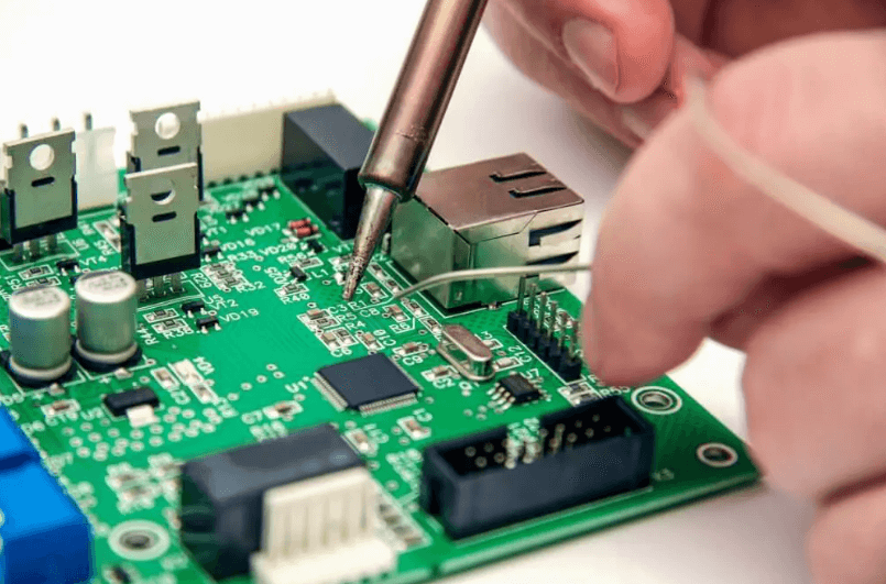
1. Physical PCB Analysis
The first step in PCB reverse engineering involves a thorough physical examination of the board:
- Visual Inspection: Documenting component placement, board dimensions, and layer count
- High-Resolution Imaging: Using specialized cameras or scanners to capture board details
- Material Analysis: Determining substrate materials, copper weights, and finish types
Advanced techniques may include X-ray imaging for examining internal layers and buried vias in multilayer boards.
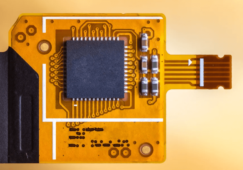
2. Component Identification and Documentation
Accurate component identification is crucial for successful reverse engineering:
- Part Number Extraction: Recording all visible markings on ICs, transistors, and passive components
- Package Measurement: Documenting physical dimensions and pin configurations
- BOM Creation: Compiling a complete bill of materials with manufacturer details
For components with erased markings, technicians may use curve tracers or signature analysis to identify parts.
3. Schematic Recreation
The core intellectual work begins with schematic recreation:
- Netlist Extraction: Tracing all electrical connections between components
- Circuit Analysis: Understanding functional blocks and signal flow
- Schematic Capture: Using EDA tools to create an accurate schematic diagram
This phase requires substantial electronics knowledge to properly interpret circuit functionality, especially for analog or mixed-signal designs.
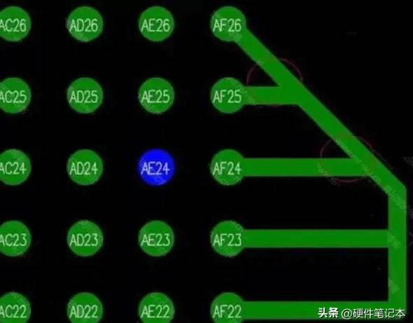
4. PCB Layout Recreation
Modern reverse engineering software assists in recreating the physical layout:
- Layer Separation: For multilayer boards, carefully separating and documenting each conductive layer
- Trace Routing: Recreating the exact copper patterns and via structures
- Design Rule Extraction: Determining clearances, trace widths, and other manufacturing parameters
Advanced tools can convert scanned images into editable PCB files through automated vectorization processes.
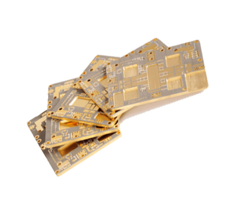
Advanced Techniques in PCB Reverse Engineering
1. Multilayer Board Processing
Complex multilayer PCBs present special challenges:
- Delamination Techniques: Carefully separating bonded layers without damage
- Layer Registration: Ensuring precise alignment when reconstructing the stackup
- Blind/Buried Via Analysis: Determining connection paths between internal layers
2. IC Decapsulation and Analysis
For comprehensive reverse engineering, component internals may be examined:
- Chemical Decapsulation: Removing package material to expose die surfaces
- Microscopy: Using optical or electron microscopes to examine chip structures
- Delayering: Progressively removing layers for complete IC analysis
3. Firmware Extraction
When dealing with populated boards with programmable components:
- Memory Dumping: Extracting firmware from flash, EEPROM, or other non-volatile memory
- Microcode Analysis: Reverse engineering processor instruction sets
- Protocol Reverse Engineering: Deciphering communication between components
Ethical Considerations and Legal Framework
1. Intellectual Property Concerns
PCB reverse engineering exists in a complex legal landscape:
- Patent Infringement: Copying patented designs may violate intellectual property laws
- Trade Secret Protection: Some designs are protected regardless of patent status
- Copyright Issues: PCB layouts may qualify as copyrighted works
2. Legitimate Use Cases
There are numerous ethical applications for PCB reverse engineering:
- Interoperability Development: Creating compatible products or accessories
- Maintenance and Repair: Supporting legacy systems when original documentation is lost
- Security Research: Identifying vulnerabilities in electronic systems
- Educational Purposes: Studying design techniques for learning
3. Industry Standards and Compliance
Professional reverse engineering services typically adhere to:
- NDA Protection: Ensuring client confidentiality
- Clean Room Design: Creating new implementations without direct copying
- Legal Review: Verifying compliance with relevant laws
Applications of PCB Reverse Engineering
1. Legacy System Support
Many industries rely on reverse engineering to maintain aging equipment:
- Military Systems: Maintaining decades-old electronics in service
- Industrial Controls: Supporting manufacturing equipment with obsolete parts
- Aerospace: Keeping avionics systems operational beyond original lifecycles
2. Competitive Analysis
Businesses use reverse engineering for market research:
- Benchmarking: Comparing product designs against competitors
- Technology Tracking: Monitoring industry trends and innovations
- Cost Reduction Analysis: Understanding manufacturing approaches
3. Failure Analysis and Quality Improvement
Reverse engineering supports product enhancement:
- Defect Investigation: Determining root causes of field failures
- Design Optimization: Identifying opportunities for improvement
- Counterfeit Detection: Verifying component authenticity
4. Security Research
Critical for identifying vulnerabilities:
- Hardware Backdoors: Detecting malicious circuit modifications
- Encryption Weaknesses: Analyzing security implementations
- Tamper Evidence: Developing protection against physical attacks
Tools and Technologies for PCB Reverse Engineering
1. Imaging and Scanning Equipment
- High-Resolution Optical Scanners: For capturing board topography
- 3D X-Ray Microscopy: For non-destructive internal inspection
- Infrared Imaging: For analyzing thermal characteristics
2. Electronic Measurement Tools
- Advanced Multimeters: For precise component characterization
- Network Analyzers: For high-frequency circuit analysis
- Logic Analyzers: For digital signal examination
3. Software Solutions
- EDA Tools: Such as Altium, Cadence, or KiCad for design recreation
- Image Processing Software: For converting scans to vector formats
- Signal Analysis Packages: For interpreting circuit behavior
4. Sample Preparation Equipment
- Precision Mills: For layer-by-layer material removal
- Plasma Etchers: For clean surface preparation
- Microscopy Stations: For detailed visual analysis
Challenges in Modern PCB Reverse Engineering
1. Increasing Design Complexity
Modern electronics present numerous challenges:
- High-Density Interconnects: Extremely fine pitch components and traces
- Embedded Components: Passives and actives within the board substrate
- Advanced Packaging: Such as wafer-level chip-scale packages
2. Security Countermeasures
Many manufacturers implement protections:
- Obfuscation Techniques: Deliberate maze-like routing patterns
- Tamper Protection: Sensors that erase data when probed
- Encrypted Firmware: Preventing code extraction and analysis
3. Legal and Ethical Boundaries
Navigating acceptable practices requires:
- Clear Documentation: Maintaining records of clean-room processes
- Legal Counsel: Ensuring compliance with relevant jurisdictions
- Ethical Guidelines: Establishing company policies for acceptable use
Future Trends in PCB Reverse Engineering
1. Automation and AI Assistance
Emerging technologies are transforming the field:
- Machine Learning Algorithms: For automated component recognition
- Image Processing AI: For faster scan-to-CAD conversion
- Predictive Circuit Analysis: Suggesting likely schematic structures
2. Advanced Imaging Technologies
New inspection methods are being developed:
- Terahertz Imaging: For non-destructive internal scanning
- Quantum Sensors: For ultra-sensitive measurements
- Atomic Force Microscopy: For nanometer-scale analysis
3. Enhanced Security Measures
The arms race continues:
- Physical Unclonable Functions: Creating unique, uncopyable identifiers
- Dynamic Circuitry: Boards that change characteristics over time
- Quantum Encryption: Future-proof security implementations
Conclusion
PCB reverse engineering remains a vital technical discipline with applications ranging from legitimate product development to critical system maintenance. As electronic devices become more complex and more integrated into every aspect of modern life, the skills and technologies involved in PCB analysis continue to evolve.
The field balances on a fine line between legitimate technical practice and intellectual property concerns, requiring practitioners to maintain high ethical standards while pushing the boundaries of technical capability. With proper attention to legal frameworks and responsible use, PCB reverse engineering will continue to serve important roles in electronics development, security research, and legacy system support for years to come.
Future advancements in automation, artificial intelligence, and advanced imaging promise to make the process more accurate and efficient, while simultaneously driving innovations in circuit protection and anti-reverse engineering techniques. This ongoing technological dialogue ensures PCB reverse engineering will remain a dynamic and challenging field at the heart of electronics innovation.