Common PCB Layout Traps and How to Avoid Them
Introduction
Printed Circuit Board (PCB) design is a complex process that requires careful attention to detail. Even experienced engineers can fall into common layout traps that lead to performance issues, manufacturing difficulties, or complete board failures. This article explores the most prevalent PCB layout pitfalls encountered in modern electronics design and provides practical solutions to avoid them.
Understanding these traps is crucial for designing reliable, manufacturable, and high-performance PCBs. We’ll examine issues related to component placement, routing, power distribution, signal integrity, thermal management, and manufacturing considerations.
1. Poor Component Placement
The Decoupling Capacitor Distance Trap
One of the most common mistakes in PCB layout is placing decoupling capacitors too far from the ICs they’re meant to protect. Decoupling capacitors need to be as close as possible to the power pins they serve to minimize parasitic inductance in the connection.
Solution:
- Place decoupling capacitors on the same side of the board as the IC
- Position them as close as possible to the power pins
- Use multiple vias when connecting to power planes
- Follow manufacturer recommendations for capacitor quantity and values
The Connector Placement Problem
Improperly placed connectors can create numerous issues:
- Forcing difficult routing paths
- Creating signal integrity problems
- Causing mechanical interference
- Making assembly and testing difficult
Solution:
- Position connectors near board edges
- Consider cable routing during placement
- Group related connectors together
- Allow sufficient clearance for mating and unmating
The Thermal Component Cluster
Placing heat-generating components too close together creates localized hot spots that can lead to thermal runaway and premature failure.
Solution:
- Spread heat-generating components across the board
- Provide adequate spacing for heat dissipation
- Consider airflow patterns in the final enclosure
- Use thermal relief patterns in copper pours
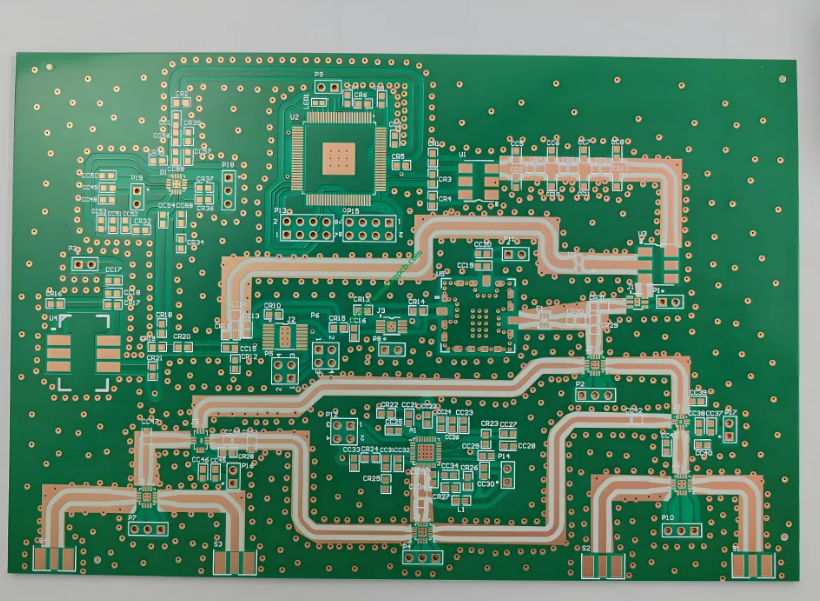
2. Routing Pitfalls
The 90-Degree Angle Myth
While modern PCB manufacturing can reliably produce 90-degree traces, these sharp angles can still cause problems:
- Potential acid traps in etching (less common with modern processes)
- Impedance discontinuities in high-frequency signals
- Increased electromagnetic radiation at corners
Solution:
- Use 45-degree angles for trace direction changes
- For very high-frequency designs, use curved traces
- Maintain consistent trace width through turns
The Via Overuse Problem
Excessive via usage can:
- Increase board cost
- Reduce reliability
- Create impedance discontinuities
- Occupy valuable routing space
Solution:
- Minimize layer transitions
- Use appropriate via sizes for current requirements
- Consider microvias for high-density designs
- Avoid via stubs in high-speed signals
The Daisy-Chain Routing Trap
Daisy-chaining signals, especially clocks and critical control signals, can cause:
- Signal integrity issues
- Timing skew problems
- Increased susceptibility to noise
Solution:
- Use star topologies for critical signals
- Implement proper bus routing for parallel signals
- Consider using buffer chips when fanout is necessary
3. Power Distribution Mistakes
The Thin Power Trace Problem
Undersized power traces can lead to:
- Excessive voltage drop
- Increased trace heating
- Power supply instability
- Reduced noise margin
Solution:
- Calculate required trace widths based on current
- Use power planes when possible
- Implement proper copper weight selection
- Consider using thicker external layers for high-current paths
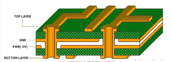
The Split Plane Resonance Issue
Improperly designed split planes can create:
- Antenna effects at certain frequencies
- Impedance discontinuities
- Increased EMI radiation
Solution:
- Avoid splitting planes when possible
- Use proper stitching techniques when splits are necessary
- Consider the return current paths when placing splits
- Use multiple vias to bridge splits for high-frequency signals
The Star Ground Illusion
Attempting to implement a “star ground” on multilayer boards often creates more problems than it solves:
- Increases loop areas
- Creates impedance mismatches
- Often impractical in modern designs
Solution:
- Implement proper ground planes
- Use partitioning wisely
- Maintain low-impedance return paths
- Consider mixed-signal grounding techniques appropriate for your frequencies
4. Signal Integrity Oversights
The Unterminated Line Problem
Neglecting proper termination for transmission lines causes:
- Signal reflections
- Ringing
- False triggering
- EMI issues
Solution:
- Identify critical transmission lines
- Implement appropriate termination (series, parallel, etc.)
- Calculate proper termination values based on trace impedance
- Consider driver strength when designing terminations
The Crosstalk Neglect
Ignoring potential crosstalk issues leads to:
- Signal integrity degradation
- Increased bit error rates
- EMI compliance problems
Solution:
- Maintain proper spacing between sensitive traces
- Use ground guards when necessary
- Route sensitive traces on different layers when possible
- Consider differential signaling for critical paths
The Return Path Discontinuity
Forgetting about signal return paths creates:
- Increased EMI
- Ground bounce
- Signal integrity problems
Solution:
- Always consider the complete current loop
- Avoid gaps in reference planes under critical traces
- Use stitching vias near high-speed signals changing layers
- Be mindful of slotting in planes
5. Manufacturing Oversights
The Silkscreen Overlap Trap
Poor silkscreen placement can:
- Cover test points or pads
- Interfere with component placement
- Create assembly confusion
Solution:
- Maintain clearance around all pads
- Keep reference designators visible
- Avoid placing text under components
- Use appropriate line widths and fonts
The Insufficient Clearance Issue
Inadequate spacing causes:
- Manufacturing yield problems
- Potential short circuits
- Difficulty in rework
Solution:
- Follow manufacturer’s design rules
- Provide extra clearance for high-voltage traces
- Consider tolerances and misregistration
- Account for solder mask expansion
The Non-Standard Hole Size Problem
Using unusual hole sizes:
- Increases fabrication cost
- May require special tooling
- Can lead to reliability issues
Solution:
- Stick to standard drill sizes when possible
- Consult with your manufacturer early
- Consider aspect ratio limitations
- Use appropriate annular ring sizes
6. Thermal Management Mistakes
The Copper Heat Island Effect
Large copper areas without thermal relief can:
- Make soldering difficult
- Create uneven heating during reflow
- Cause tombstoning of small components
Solution:
- Use thermal relief connections for pads
- Balance copper distribution
- Consider solder mask defined pads for small components
- Follow manufacturer’s recommendations for thermal design
The Ventilation Oversight
Neglecting proper airflow leads to:
- Component overheating
- Reduced reliability
- Performance degradation
Solution:
- Consider component placement for natural convection
- Provide adequate spacing for airflow
- Use thermal vias under hot components
- Consider the entire system’s thermal design
7. Test and Debugging Oversights
The Missing Test Point Problem
Failing to include test points makes:
- Prototype debugging difficult
- Production testing challenging
- Field service nearly impossible
Solution:
- Add test points for critical signals
- Provide adequate clearance around test points
- Consider automated test requirements early
- Document test point locations and purposes
The Inaccessible Component Trap
Placing components where they can’t be probed or replaced:
- Complicates debugging
- Makes rework difficult
- Increases repair costs
Solution:
- Leave space around components that may need probing
- Consider probe access during layout
- Avoid placing tall components near those needing service
- Document any special access requirements
Conclusion
PCB layout is a complex balancing act that requires consideration of electrical, mechanical, thermal, and manufacturing requirements simultaneously. By being aware of these common traps and implementing the suggested solutions, designers can significantly improve their PCB quality and reliability.
The key to avoiding layout pitfalls lies in:
- Thorough planning before starting the layout
- Continuous verification during the design process
- Collaboration with manufacturing partners
- Learning from past design reviews and testing
Remember that every design is unique, and what works for one project may not be optimal for another. Develop a checklist based on these common traps and adapt it to your specific design requirements. With careful attention to these details, you can avoid the most common PCB layout traps and create robust, reliable circuit boards.