Premier PCB Assembly Services for Cutting-Edge Electronics

Key Takeaways
Selecting the right PCB assembly partner requires balancing technical expertise, scalability, and adherence to stringent quality standards. Leading providers specialize in PCBA solutions tailored for industries like aerospace, IoT, and medical technology, where precision and reliability are non-negotiable. For aerospace applications, military-grade certifications and thermal management capabilities often differentiate top-tier manufacturers. In IoT development, firms offering high-density interconnect (HDI) boards and flexible PCB designs enable seamless integration with compact, connected devices.
"Partnering with a PCB assembly company that offers advanced prototyping ensures faster iteration cycles, reducing time-to-market for mission-critical electronics."
When evaluating options, prioritize suppliers with proven expertise in ISO 13485-compliant processes for medical devices or AS9100D certification for aerospace projects. High-volume production demands facilities equipped with automated optical inspection (AOI) and surface-mount technology (SMT) lines to maintain consistency across large batches. For specialized insights into optimizing PCBA workflows, explore Nelson Design’s PCB manufacturing resources, which detail best practices for design-for-manufacturability (DFM) and testing protocols.
Ultimately, the ability to scale from prototyping to full-scale production while maintaining zero-defect benchmarks remains a hallmark of industry-leading PCB assembly services.
Top PCB Assembly Firms for Aerospace Tech
Aerospace systems demand PCB assembly solutions capable of enduring extreme temperatures, radiation, and mechanical stress while maintaining flawless performance. Leading PCBA providers serving this sector combine military-grade compliance with high-density interconnect (HDI) technologies to meet stringent aerospace standards like IPC-610 Class 3 and AS9100D. These firms specialize in manufacturing multilayer boards with embedded components, ensuring reliability for avionics, satellite communications, and navigation systems. For example, MicroArt Services employs automated optical inspection (AOI) and X-ray testing to validate solder joints and component alignment, critical for mission-critical applications. Advanced thermal management techniques, such as ceramic substrates or metal-core PCBs, further enhance durability in high-vibration environments. By integrating traceability protocols and supply chain resilience, top-tier PCB assembly partners mitigate risks in aerospace projects, from prototyping to full-scale production. Their expertise in conformal coating and hermetic sealing ensures long-term functionality even in low-pressure or corrosive atmospheres, aligning with the aerospace industry’s zero-failure ethos.

Precision PCB Solutions for IoT Innovations
The rapid evolution of IoT (Internet of Things) devices demands PCB assembly processes that prioritize miniaturization, energy efficiency, and signal integrity. Leading PCBA providers leverage advanced techniques like laser-drilled microvias and embedded component technology to meet these requirements, ensuring seamless integration with sensors, wireless modules, and low-power processors. For IoT applications—from smart agriculture to industrial automation—precision in PCB assembly directly impacts device reliability in harsh environments.
A critical focus lies in optimizing designs for thermal management and RF performance, particularly for wearables and edge-computing nodes. Below is a comparison of key considerations for IoT-optimized PCBA:
| Feature | Standard PCB | IoT-Optimized PCB |
|---|---|---|
| Layer Count | 4-6 layers | 6-12 layers (HDI) |
| Material | FR-4 | High-frequency laminates |
| Component Density | ≤ 50/cm² | ≥ 100/cm² |
| Testing Protocols | Basic functional tests | EMI/ESD compliance checks |
To achieve cost-effective scaling without compromising quality, manufacturers adopt automated optical inspection (AOI) and X-ray verification during PCB assembly. For insights on balancing budget and performance, explore best practices here. As IoT ecosystems expand, partnerships with PCBA specialists skilled in flexible substrates and ultra-fine-pitch soldering become indispensable for innovators aiming to lead in connected-device markets.
Leading Medical Electronics Assembly Services
Modern medical devices demand PCB assembly processes that meet stringent regulatory and performance requirements. From implantable sensors to diagnostic equipment, precision and reliability are non-negotiable in medical-grade PCBA. Leading providers leverage automated optical inspection (AOI) and X-ray testing to ensure traceability and compliance with ISO 13485 and FDA standards. For example, advanced flexible circuits and high-density interconnects enable compact designs for wearable health monitors, while biocompatible materials ensure safety in long-term implants.
Scalability is equally critical, as medical innovators often transition from low-volume prototyping to full-scale production. Partnering with a qualified PCB assembly specialist ensures seamless integration of mixed-technology components—such as fine-pitch BGAs and microcontrollers—without compromising on defect rates. This is particularly vital for life-saving devices like infusion pumps or cardiac monitors, where zero-defect manufacturing directly impacts patient outcomes.
In applications ranging from telemedicine to robotic surgery, medical electronics PCBA requires a balance of innovation and adherence to risk management frameworks. By prioritizing traceable supply chains and cleanroom assembly, top-tier manufacturers deliver solutions that align with the evolving demands of global healthcare systems.
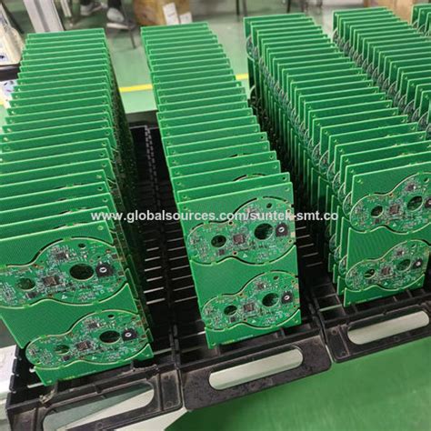
High-Volume PCB Production for Scalable Demands
Meeting high-volume PCB assembly demands requires a seamless blend of advanced manufacturing technologies and robust supply chain management. Leading PCBA providers leverage automated production lines equipped with surface-mount technology (SMT) and through-hole assembly systems to ensure consistent output for industries like automotive, consumer electronics, and industrial automation. These systems enable rapid scaling from prototype batches to millions of units while maintaining near-zero defect rates through AI-driven quality inspection protocols.
Critical to scalability is the integration of just-in-time (JIT) inventory practices, which minimize lead times without compromising material traceability. Top-tier PCB assembly firms employ enterprise resource planning (ERP) platforms to synchronize component procurement, assembly workflows, and testing cycles, ensuring alignment with fluctuating market demands. For sectors requiring stringent compliance—such as aerospace or medical devices—vendors combine ISO 9001-certified processes with IPC-A-610 Class 3 standards to guarantee reliability under extreme conditions.
By prioritizing flexible manufacturing ecosystems, PCBA specialists empower clients to adapt to evolving production scales, whether ramping up for seasonal peaks or supporting long-term IoT infrastructure expansions. This agility, paired with rigorous quality assurance frameworks, positions high-volume PCB production as a cornerstone for next-generation electronic innovations.
Advanced Prototyping in PCB Manufacturing
In the realm of PCB assembly, advanced prototyping serves as the cornerstone for transforming conceptual designs into functional electronics. Leading PCBA providers leverage state-of-the-art tools like 3D modeling software and automated optical inspection (AOI) to accelerate iterative testing, ensuring seamless compatibility with cutting-edge applications in aerospace, IoT, and medical devices. By integrating rapid-turn prototyping with multi-layer board fabrication, engineers can identify and resolve potential flaws in circuitry or component placement before full-scale production.
Modern prototyping workflows emphasize design-for-manufacturability (DFM) principles, optimizing layouts for thermal management, signal integrity, and miniaturization. This phase often incorporates mixed-technology assemblies, combining surface-mount (SMT) and through-hole components to meet diverse performance criteria. For high-complexity projects, such as implantable medical sensors or satellite communication systems, PCBA partners utilize advanced materials like polyimide substrates or low-loss dielectrics to ensure reliability under extreme conditions.
Transitioning from prototyping to mass production requires meticulous validation, including thermal cycling tests and functional simulations. These steps not only reduce time-to-market but also align with the broader article themes of scalability and precision across critical industries.
Industry-Leading Electronics Assembly Standards
Modern electronics demand PCB assembly processes that adhere to rigorous quality benchmarks, particularly for industries where reliability is non-negotiable. Leading PCBA providers implement ISO 9001 and IPC-A-610 certifications as foundational frameworks, ensuring every solder joint, component placement, and layer alignment meets exacting specifications. These standards are critical in applications like aerospace systems, where temperature fluctuations and vibration resistance directly impact performance.
Advanced manufacturers leverage automated optical inspection (AOI) and X-ray testing to detect microscopic defects, minimizing failure risks in mission-critical devices. For high-density interconnect (HDI) boards, precision becomes even more vital, requiring specialized equipment to manage ultra-fine pitch components. Additionally, traceability systems are integrated into PCB assembly workflows, enabling real-time monitoring of production batches—a necessity for medical devices requiring full compliance with FDA or CE regulations.
By combining cutting-edge technology with standardized protocols, top-tier PCBA firms ensure scalability without compromising quality. This approach not only accelerates time-to-market for IoT and industrial automation solutions but also establishes trust for partnerships in sectors where even minor deviations carry significant consequences.

Cutting-Edge PCB Tech for Medical Devices
The medical electronics sector demands unparalleled precision and reliability, driving PCB assembly providers to innovate with specialized technologies. Modern PCBA processes for medical devices prioritize miniaturization and biocompatibility, enabling compact designs for implantable monitors, diagnostic tools, and wearable health trackers. Advanced substrates like polyimide flex circuits and high-frequency laminates ensure durability in sterilization cycles and compatibility with sensitive biological environments.
To meet stringent regulatory standards such as ISO 13485, leading manufacturers integrate automated optical inspection (AOI) and X-ray testing into their PCB assembly workflows. These protocols detect micro-defects in high-density interconnect (HDI) boards, critical for devices like MRI systems and infusion pumps. Additionally, thermally optimized layouts prevent overheating in prolonged-use equipment, while embedded sensors enable real-time performance monitoring.
Collaboration between medical engineers and PCBA experts is vital for prototyping life-saving technologies, from neural interfaces to portable dialysis machines. By leveraging laser-drilled microvias and ultra-fine pitch components, suppliers achieve the signal integrity required for low-noise data transmission in ECG or EEG devices. This synergy of innovation and compliance ensures medical electronics meet both technical and ethical benchmarks, seamlessly aligning with the industry’s shift toward smart, patient-centric solutions.
Trusted PCB Partners for Critical Applications
Selecting PCB assembly partners for mission-critical systems demands rigorous evaluation of technical expertise and quality assurance protocols. Industries like aerospace, medical device manufacturing, and defense rely on PCBA providers capable of adhering to zero-defect standards while navigating complex regulatory landscapes. Leading firms distinguish themselves through certifications such as ISO 13485 (medical devices) and AS9100D (aerospace), ensuring traceability and compliance with stringent safety requirements.
For applications where failure is not an option, advanced PCB assembly workflows integrate automated optical inspection (AOI) and X-ray testing to detect microscopic flaws. Partners specializing in high-reliability mixed-technology assemblies—combining surface-mount (SMT) and through-hole components—prove indispensable for ruggedized electronics in extreme environments. Transitioning to automated assembly becomes critical when scaling production without compromising precision, particularly for multilayer boards with fine-pitch components.
Trusted collaborators also offer risk-mitigation strategies, including component lifecycle management and counterfeit part avoidance programs, to safeguard supply chains for long-duration projects. By aligning with PCBA providers that prioritize failure mode analysis (FMA) and real-time production monitoring, manufacturers ensure their mission-critical systems meet both performance benchmarks and lifecycle durability expectations.
Conclusion
Selecting the right PCB assembly partner is critical for industries demanding precision, reliability, and scalability. As aerospace, IoT, and medical device sectors push technological boundaries, PCBA providers must balance advanced prototyping capabilities with rigorous quality control to meet evolving standards. Leading firms differentiate themselves through cutting-edge manufacturing processes, including automated optical inspection (AOI) and surface-mount technology (SMT), ensuring seamless integration of complex components.
For mission-critical applications, adherence to industry-specific certifications—such as ISO 13485 for medical devices or AS9100 for aerospace—remains non-negotiable. Meanwhile, high-volume production demands agile supply chain management and DFM (Design for Manufacturing) optimization to minimize lead times without compromising performance. By prioritizing collaboration with PCB assembly specialists who invest in R&D and sustainable practices, businesses can future-proof their electronics while maintaining compliance with global regulatory frameworks. Ultimately, the convergence of innovation and operational excellence defines success in today’s fast-paced electronics landscape.
Frequently Asked Questions
What factors differentiate top-tier PCB assembly providers from standard services?
Leading PCBA suppliers distinguish themselves through AS9100D certification for aerospace applications, ISO 13485-compliant processes for medical devices, and AI-driven quality control systems. They prioritize traceability across production batches and offer flexible scalability from 10 to 100,000+ units.
How do PCB assembly timelines vary between prototyping and high-volume orders?
Prototyping typically requires 5–7 days for PCBA completion, while high-volume orders demand 2–4 weeks due to multilayer board complexity and rigorous testing protocols. Accelerated options exist for urgent IoT or automotive projects.
What industries benefit most from specialized PCB assembly solutions?
Aerospace systems require high-reliability PCBA designs with MIL-STD-883 shock resistance, while medical tech demands biocompatible coatings and FDA-approved materials. IoT developers rely on ultra-compact layouts for wearable integrations.
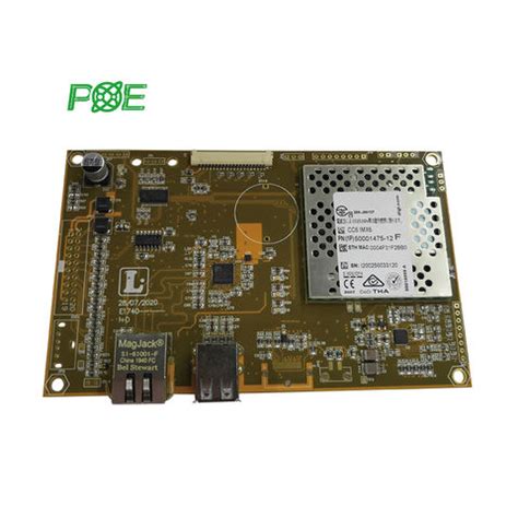
Can PCB assembly firms handle mixed-technology boards with HDI and flexible circuits?
Advanced providers support hybrid designs combining rigid-flex boards, microvia architectures, and 01005-sized components. This capability is critical for miniaturized medical implants and aerospace avionics.
Why is design-for-manufacturability (DFM) analysis crucial in PCBA workflows?
DFM checks prevent signal integrity issues and thermal mismatches, reducing post-production revisions by up to 65%. Top firms automate this process using 3D modeling tools and real-time collaboration platforms.
Ready to Optimize Your Next PCB Assembly Project?
Leverage cutting-edge PCBA solutions tailored for your industry’s demands. Click here to explore precision manufacturing options or request a free design consultation today.