Why Do PCBs Short Circuit? Causes, Prevention, and Solutions
Introduction
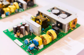
Printed Circuit Boards (PCBs) form the backbone of modern electronics, found in everything from smartphones to industrial machinery. A short circuit (or “short”) in a PCB occurs when an unintended low-resistance connection forms between two points in a circuit that should not be connected, causing current to flow along an undesired path. PCB shorts can range from minor annoyances to catastrophic failures that destroy entire systems. Understanding why these shorts occur is essential for designers, manufacturers, and technicians working with electronic systems.
This article explores the various causes of PCB short circuits, methods for prevention, and techniques for troubleshooting when shorts occur. We’ll examine design-related causes, manufacturing defects, environmental factors, and operational issues that contribute to this common but problematic phenomenon in electronics.
Section 1: Design-Related Causes of PCB Shorts
1.1 Inadequate Clearance and Creepage Distances
One of the most fundamental causes of PCB shorts stems from insufficient spacing between conductive elements. Designers must maintain proper:
- Clearance: The shortest air distance between two conductors
- Creepage: The shortest path along a surface between conductors
Industry standards like IPC-2221 provide guidelines for these distances based on voltage levels. When designers ignore these standards or attempt to miniaturize circuits excessively, the risk of arcing or conductive filament formation increases dramatically.
1.2 Improper Trace Routing
Poor routing practices frequently lead to shorts:
- Acute angle traces: These can cause acid traps during etching, leading to unintended copper connections
- Parallel high-voltage traces: These may induce capacitive coupling or arcing
- Insufficient power/ground planes: Can force current through unintended paths
1.3 Component Placement Errors
Even with perfect routing, poor component placement can cause shorts:
- Overlapping footprints: Components physically interfering with each other
- Inadequate spacing for heat dissipation: Thermal expansion causing contact
- High-density areas without proper isolation: Increased risk of solder bridging
Section 2: Manufacturing Defects Leading to Shorts
2.1 Etching Problems
The PCB etching process removes unwanted copper, but several issues can occur:
- Under-etching: Incomplete copper removal leaves conductive strands
- Over-etching: Can weaken traces, leading to breaks that cause secondary shorts
- Uneven etching: Creates thin copper hairs that may bridge gaps
2.2 Solder-Related Issues
Soldering defects account for a significant percentage of PCB shorts:
- Solder bridges: Excess solder connecting adjacent pads or pins (common in QFP and BGA packages)
- Solder balls: Tiny spheres that can roll and create random connections
- Whiskers: Metallic growths that form over time between close conductors
2.3 Contamination and Foreign Materials
Even microscopic contaminants can cause shorts:
- Metallic debris: From machining or handling can create conductive paths
- Conductive dust: Carbon or metal particles accumulating in humid environments
- Flux residues: Some no-clean fluxes become conductive when contaminated
Section 3: Environmental and Operational Causes
3.1 Moisture and Humidity
Water is an excellent conductor when contaminated with ions:
- Electrochemical migration: Metal ions dissolve and redeposit as dendrites
- Conductive anodic filaments (CAF): Copper grows through the laminate along glass fibers
- Corrosion: Can create unintended conductive paths between traces
3.2 Thermal Stress and Cycling
Repeated heating and cooling causes:
- Substrate warping: Can force components into contact
- Solder joint fatigue: May cause components to shift position
- Laminate degradation: Breakdown of insulating materials
3.3 Mechanical Stress and Physical Damage
Physical impacts create multiple shorting scenarios:
- Flex cracks: Broken traces that contact other layers
- Component displacement: Parts knocked out of position
- Delamination: Separation of PCB layers creating unintended contact
Section 4: Identifying and Troubleshooting PCB Shorts
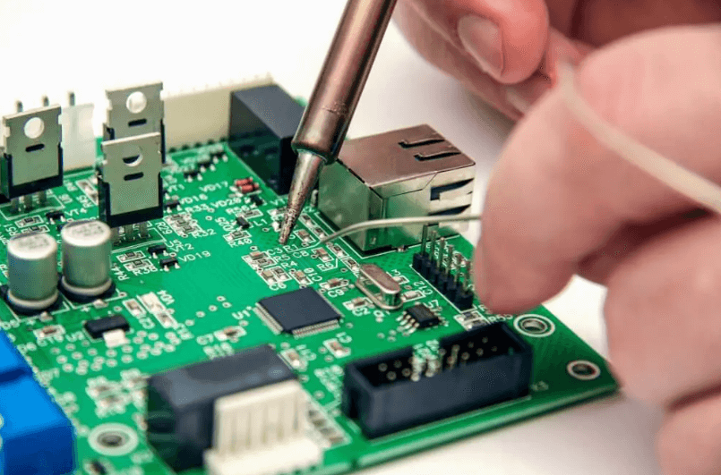
4.1 Visual Inspection Techniques
Many shorts are visible under proper lighting and magnification:
- Microscopic examination: 10-30x magnification often reveals solder bridges
- Angled lighting: Helps spot raised conductive filaments
- Infrared imaging: Shows heat patterns from current leakage
4.2 Electrical Testing Methods
Several tools help locate shorts electrically:
- Continuity testing: Basic check for unexpected connections
- Milliohm meters: Measure very low resistance paths
- Time-domain reflectometry (TDR): Pinpoints short locations by signal reflection
4.3 Advanced Diagnostic Approaches
For complex multilayer boards:
- X-ray inspection: Reveals internal layer shorts
- Thermal imaging: Identifies current leakage paths
- Acoustic microscopy: Detects subsurface anomalies
Section 5: Prevention and Best Practices
5.1 Design for Manufacturing (DFM) Principles
Incorporating manufacturability reduces short risks:
- Follow IPC standards for clearances and tolerances
- Include testability features like test points and breakout circuits
- Simulate manufacturing processes to identify potential issues
5.2 Quality Control in Manufacturing
Robust QC prevents many shorts:
- Automated Optical Inspection (AOI): Catches visible defects
- Electrical testing: 100% continuity and isolation testing
- Process controls: Monitor etching, soldering, and cleaning parameters
5.3 Environmental Protection
Shielding PCBs from harsh conditions:
- Conformal coatings: Protect against moisture and contamination
- Proper enclosures: Prevent physical damage and dust accumulation
- Humidity controls: For storage and operation environments
Conclusion
PCB short circuits arise from a complex interplay of design decisions, manufacturing processes, environmental conditions, and operational stresses. While some shorts result from obvious errors like solder bridges, others develop gradually through electrochemical processes or mechanical fatigue. Modern PCB complexity, with high-density interconnects and multilayer architectures, has only increased the potential for short circuits.
Preventing shorts requires a holistic approach encompassing robust design practices, controlled manufacturing processes, proper handling procedures, and appropriate operating environments. When shorts do occur, systematic troubleshooting using both visual and electrical techniques can efficiently locate and rectify the issues.
As electronics continue advancing toward smaller form factors and higher performance, understanding and mitigating PCB short circuits remains a critical challenge for the industry. Ongoing developments in materials science, manufacturing technologies, and design tools continue to provide new solutions to this persistent problem in electronic systems.