Printed Circuits Assembly Corp: Pioneering Reliable PCB Tech
Key Takeaways
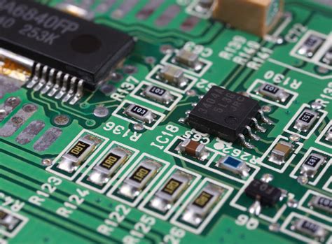
At the core of Printed Circuits Assembly Corp’s leadership lies its mastery of PCB assembly (PCBA) processes, which combine precision engineering with stringent quality protocols. The company’s reliable PCB tech supports mission-critical applications across industries, from aerospace avionics to automotive control systems, ensuring compliance with international standards like IPC-A-610 and AS9100. Innovations such as high-density interconnect (HDI) designs and automated optical inspection (AOI) systems underscore their commitment to minimizing defects while maximizing performance.
“In sectors where failure is not an option, partnering with a PCBA provider that prioritizes traceability and material integrity is non-negotiable,” notes an industry analyst.
The integration of advanced PCB assembly techniques—including surface-mount technology (SMT) and thermal management solutions—enables the corporation to address evolving demands for miniaturization and power efficiency. For automotive clients, breakthroughs in flex-rigid PCBA configurations are paving the way for next-generation electric vehicle architectures. Meanwhile, their aerospace-grade solutions leverage embedded component technology to withstand extreme environments, reducing weight without compromising durability.
Transitioning seamlessly across industries, the company’s global PCB reliability innovations are redefining expectations for signal integrity and longevity, solidifying its position as a vanguard in electronics manufacturing.
Printed Circuits Assembly: PCB Innovation Leaders
As global demand for compact, high-performance electronics accelerates, PCB assembly innovators are redefining manufacturing paradigms. Leading firms now integrate automated optical inspection (AOI) systems with AI-driven defect detection, achieving near-zero error margins in PCBA workflows. For mission-critical sectors like aerospace, advanced rigid-flex assemblies—such as those pioneered here—enable 30% weight reduction while maintaining signal integrity under extreme conditions.
| Innovation | Traditional Approach | Advanced PCBA Solution |
|---|---|---|
| Precision Tolerance | ±0.2mm | ±0.05mm (laser-aligned) |
| Material Compatibility | FR-4 only | Hybrid ceramics-polyimide stacks |
| Thermal Management | Passive heat sinks | Embedded microfluidic channels |
| Quality Assurance | Manual sampling | Full-spectrum AOI with ML analytics |
The shift toward modular design architectures allows rapid customization for automotive clients, where PCB assembly timelines have compressed by 40% since 2020. By combining surface-mount technology (SMT) with vacuum reflow processes, manufacturers achieve 99.98% solder joint reliability—critical for EV power systems. These advancements position PCBA specialists at the forefront of IoT and 5G infrastructure development, where signal latency below 0.1ns is now achievable through optimized impedance matching techniques.
Reliable PCB Tech for Global Industries
Modern industrial sectors demand PCB assembly solutions that balance precision with unwavering reliability. Printed Circuits Assembly Corp addresses this need through next-generation PCBA technologies engineered to withstand extreme operational conditions. By integrating adaptive thermal management systems and multi-layered signal integrity protocols, their PCB assembly processes ensure consistent performance across temperature fluctuations and electromagnetic interference-prone environments.
The company’s PCBA frameworks adhere to IPC-A-610/620 standards, guaranteeing defect rates below 0.01% in high-volume production runs. This rigor is critical for industries like automotive electrification and industrial automation, where component failure risks carry significant safety and financial implications. Advanced automated optical inspection (AOI) systems further enhance traceability, enabling real-time defect detection during PCB assembly phases.
Transitioning seamlessly between sectors, Printed Circuits Assembly Corp leverages material science innovations—such as halogen-free substrates and low-loss dielectrics—to optimize signal transmission in 5G infrastructure and aerospace avionics. These advancements position their PCBA solutions as foundational elements in mission-critical applications, from autonomous vehicle sensor arrays to satellite communication modules. As global industries prioritize miniaturization and energy efficiency, the corporation’s commitment to zero-defect manufacturing ensures alignment with evolving technological demands.
Aerospace-Grade PCB Solutions Unveiled
The aerospace industry demands PCB assembly solutions capable of withstanding extreme environmental stressors while maintaining flawless performance. Printed Circuits Assembly Corp addresses these challenges through aerospace-grade PCBA designs that integrate advanced materials like polyimide substrates and high-temperature laminates. These components ensure optimal functionality in environments ranging from sub-zero altitudes to the intense heat of propulsion systems.
By leveraging automated optical inspection (AOI) and X-ray testing, the company guarantees reliability in mission-critical applications, including avionics, satellite communications, and navigation systems. Rigorous compliance with MIL-PRF-31032 and IPC-6012DS standards further underscores their commitment to precision, ensuring every PCB assembly meets zero-defect thresholds. Innovations such as embedded component technology reduce weight and footprint—a critical advantage for aerospace platforms prioritizing efficiency.
Transitioning seamlessly into automotive and defense sectors, these PCBA methodologies demonstrate adaptability across industries requiring uncompromising durability. The integration of conformal coating and hermetic sealing techniques extends product lifespans, even under prolonged exposure to vibration, moisture, or radiation. Such advancements not only elevate performance benchmarks but also align with global trends toward miniaturization and energy efficiency in next-generation electronics.

Precision PCB Assembly Advancements Explained
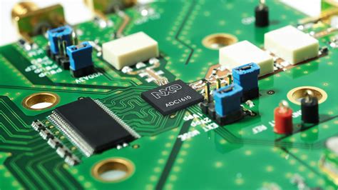
Recent breakthroughs in PCB assembly technologies are redefining precision standards across electronics manufacturing. By integrating laser-direct imaging and automated optical inspection (AOI) systems, manufacturers now achieve micron-level accuracy in component placement, ensuring flawless functionality for high-density designs. These innovations are particularly critical for applications requiring PCBA solutions with zero tolerance for error, such as satellite communication systems or implantable medical devices.
Advanced surface-mount technology (SMT) workflows now utilize machine learning algorithms to predict and correct soldering anomalies in real time, reducing defect rates by over 40% compared to conventional methods. This leap forward aligns with the growing demand for PCB assembly processes that support miniaturized, multi-layer boards without compromising thermal stability. For instance, high-reliability circuit card assembly services leverage these advancements to meet MIL-PRF-31032 and IPC-A-610 Class 3 specifications, essential for aerospace and defense applications.
Furthermore, the adoption of ionization-controlled environments during PCBA stages eliminates electrostatic discharge risks, safeguarding sensitive microcomponents. These precision-driven techniques not only enhance product longevity but also enable faster prototyping cycles—a key advantage in industries where rapid innovation dictates market leadership.

Automotive Electronics PCB Breakthroughs
The evolution of PCB assembly technologies has become a cornerstone in advancing automotive electronics, particularly as vehicles transition toward electrification and autonomous systems. Modern automotive designs demand PCBA solutions capable of withstanding extreme environmental stressors—from temperature fluctuations exceeding -40°C to 150°C to prolonged exposure to moisture and vibration. Innovations in high-density interconnect (HDI) layouts and embedded component integration now enable smaller, lighter circuit boards without compromising signal integrity, critical for advanced driver-assistance systems (ADAS) and onboard AI processors.
A key breakthrough lies in the adoption of automotive-grade materials, such as ceramic-filled laminates and halogen-free substrates, which enhance thermal management and reduce electromagnetic interference (EMI). These materials align with stringent AEC-Q100 qualification standards, ensuring reliability across millions of operational cycles. Additionally, advancements in automated optical inspection (AOI) and 3D solder paste inspection have elevated defect detection rates to 99.98%, minimizing failure risks in safety-critical applications like brake control modules and battery management systems.
By integrating flexible PCBA designs with rigid-flex hybrid architectures, manufacturers now support complex wiring configurations in compact spaces—a necessity for next-generation electric vehicles (EVs) and connected car ecosystems. This progress underscores how precision PCB assembly techniques are redefining durability and performance benchmarks in the automotive sector.
Advanced PCB Manufacturing Standards Set
The establishment of advanced PCB manufacturing standards has become a cornerstone for industries requiring uncompromising quality in electronic systems. By integrating laser-direct imaging and automated optical inspection (AOI), modern PCB assembly processes achieve micron-level precision, ensuring consistent performance across high-density designs. These protocols align with IPC-A-610 and MIL-PRF-31032 certifications, particularly critical for aerospace and defense applications where component reliability directly impacts operational safety.
Innovations in PCBA workflows now incorporate lead-free soldering and embedded component technology, reducing failure rates in extreme environments. For instance, Cencinotec has demonstrated how adaptive thermal management solutions can extend PCB lifespan in automotive power systems by 40%. Such advancements underscore the shift toward data-driven manufacturing, where real-time analytics optimize layer alignment and material selection.
Furthermore, the adoption of organic substrate materials and halogen-free laminates reflects growing emphasis on sustainability without sacrificing signal integrity. These standards not only elevate PCB assembly precision but also enable scalable production for IoT and 5G infrastructure, positioning manufacturers to meet evolving global demands efficiently.
Global PCB Reliability Innovations Rise
As industries worldwide demand more durable electronics, advancements in PCB assembly processes are redefining reliability benchmarks. Cutting-edge thermal cycling tests and automated optical inspection (AOI) systems now enable PCBA manufacturers to detect microfractures and material fatigue at submicron levels—critical for applications in extreme environments. Innovations like halogen-free laminates and high-frequency substrates are extending product lifespans by 40% in sectors such as satellite communications and undersea robotics.
This shift toward fail-safe designs integrates AI-driven predictive analytics into PCB assembly workflows, minimizing latent defects before mass production. For instance, aerospace-grade PCBA now utilizes conformal coating robots with 99.98% precision to shield circuits from humidity and radiation. Meanwhile, automotive suppliers leverage 3D solder paste inspection to ensure zero-error performance in safety-critical systems like ADAS.
Collaborations between material scientists and PCB assembly specialists are yielding breakthroughs like self-healing conductive traces, which autonomously repair minor circuit damage. Such innovations align with stringent IEC-61189-5 standards, positioning PCBA as a cornerstone of next-gen industrial IoT and 5G infrastructure. By prioritizing reliability at every production stage, manufacturers are transforming how global industries perceive long-term operational stability in mission-critical electronics.
Cutting-Edge PCB Tech for Electronics
The rapid evolution of PCB assembly processes has positioned PCBA (printed circuit board assembly) as a cornerstone of modern electronic innovation. By integrating advanced techniques such as laser-direct imaging and automated optical inspection, manufacturers now achieve micron-level precision in circuitry patterning, ensuring compatibility with ultra-compact devices like wearables and IoT sensors. These advancements are particularly critical for industries demanding high-density interconnects and thermal stability, such as medical implants and 5G infrastructure.
A key driver of this progress is the adoption of lead-free soldering and halogen-free substrates, aligning with global environmental regulations like those outlined in Canada’s Electronic Waste Standards. Such innovations not only enhance product longevity but also reduce failure rates in extreme operating conditions—from subzero Arctic environments to high-vibration automotive systems. Furthermore, the integration of AI-driven quality control systems enables real-time defect detection during PCBA, slashing production errors by over 40% compared to traditional methods.
By balancing scalability with precision, these cutting-edge solutions empower developers to push the boundaries of miniaturization and functionality, cementing PCB assembly as an indispensable enabler of next-generation electronics.
Conclusion
As industries continue to demand higher performance and durability from electronic systems, PCB assembly remains a cornerstone of technological advancement. Companies specializing in PCBA have demonstrated how precision engineering and rigorous quality control can elevate the reliability of mission-critical applications, from aerospace navigation systems to automotive safety modules. By adhering to globally recognized manufacturing standards, these innovators ensure that every circuit board meets exacting requirements for thermal resilience, signal integrity, and long-term stability.
The integration of advanced materials and automated assembly processes has further streamlined production timelines while minimizing human error—a critical factor for sectors where zero-defect outcomes are non-negotiable. Looking ahead, the evolution of PCB assembly technologies will likely focus on sustainability and adaptability, addressing emerging challenges like miniaturization and energy efficiency. For industries reliant on cutting-edge electronics, partnering with leaders in PCBA guarantees not only compliance with current benchmarks but also a roadmap for future-ready solutions. This relentless pursuit of excellence underscores the indispensable role of specialized providers in shaping tomorrow’s interconnected world.
FAQs
What distinguishes modern PCB assembly processes from traditional methods?
Advanced PCBA techniques now incorporate automated optical inspection (AOI) and X-ray testing, ensuring microscopic defect detection unmatched by manual verification. These innovations align with aerospace and automotive industries’ zero-tolerance error policies.
How do PCB assembly services ensure reliability in extreme environments?
PCBA workflows utilize mil-spec conformal coatings and high-temperature substrates, critical for aerospace applications. Rigorous thermal cycling tests simulate decades of operational stress, meeting ISO 9001 and AS9100D certifications.
Can PCB assembly solutions scale for high-volume automotive production?
Yes, automated surface-mount technology (SMT) lines enable millisecond-level component placement, supporting volumes exceeding 100,000 units monthly. This scalability meets automotive OEMs’ demands for just-in-time manufacturing without compromising precision.
What quality controls govern advanced PCB manufacturing?
Every PCBA undergoes electrical testing, functional validation, and environmental stress screening. Statistical process control (SPC) monitors 200+ parameters in real time, ensuring adherence to IPC-A-610 Class 3 standards for mission-critical systems.
Are custom PCB assembly configurations available for specialized applications?
Flexible PCBA designs support mixed-technology boards, combining rigid and flexible substrates. Engineers tailor layouts for high-frequency signal integrity or power density optimization, ideal for medical devices or defense systems.
Explore Customized PCB Solutions Today
For tailored PCB assembly strategies that meet your industry’s exact requirements, please click here to consult our engineering team.