Hidden Design Pitfalls in PCB Design: Critical Challenges and Solutions
Introduction
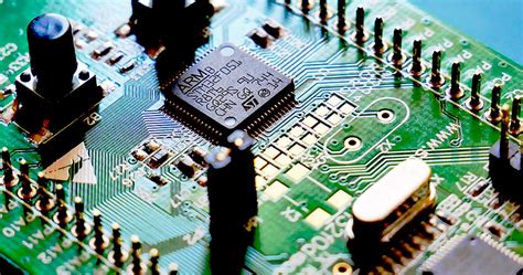
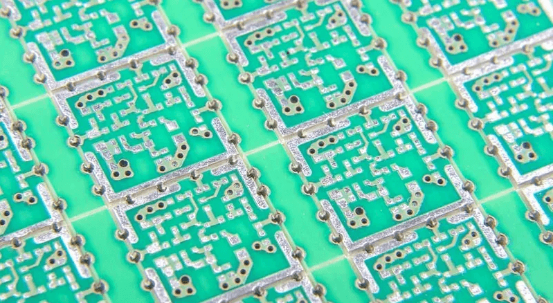
Printed Circuit Board (PCB) design is a complex process that requires meticulous attention to detail. While many designers focus on obvious aspects like component placement and routing, several subtle yet critical pitfalls can lead to circuit failures, signal integrity issues, and manufacturing defects. This article explores some of the most significant yet often overlooked design hazards in PCB development, offering insights into their causes and mitigation strategies.
1. Signal Integrity and EMI/EMC Issues
Problem:
High-speed digital circuits and RF designs are particularly susceptible to signal integrity (SI) and electromagnetic interference (EMI) problems. Poor trace routing, improper grounding, and inadequate shielding can lead to crosstalk, reflections, and radiated emissions.
Common Pitfalls:
- Impedance Mismatch: Traces carrying high-frequency signals must maintain controlled impedance. Discrepancies due to incorrect trace width or dielectric material can cause signal reflections.
- Crosstalk: Parallel routing of high-speed signals without sufficient spacing induces unwanted coupling.
- Ground Loops: Poor grounding strategies create return path discontinuities, increasing noise susceptibility.
Solutions:
- Use controlled impedance routing with proper dielectric stack-up.
- Maintain 3W rule (trace spacing ≥ 3× trace width) to minimize crosstalk.
- Implement split ground planes for mixed-signal designs but ensure proper stitching vias.
2. Power Integrity and Decoupling Challenges
Problem:
Modern PCBs with high-speed processors and FPGAs demand stable power delivery networks (PDNs). Poor power distribution leads to voltage drops, ground bounce, and transient noise.
Common Pitfalls:
- Inadequate Decoupling: Missing or poorly placed decoupling capacitors result in high-frequency noise.
- Insufficient Power Plane Design: Thin power traces or lack of solid power planes increase IR drop.
- Via Starvation: High-current paths with insufficient vias cause localized heating.
Solutions:
- Place multiple decoupling capacitors (bulk, mid-range, and high-frequency) near ICs.
- Use low-impedance power planes with proper via stitching.
- Perform PDN simulation to verify voltage stability under load.
3. Thermal Management Oversights
Problem:
Overheating reduces component lifespan and can cause intermittent failures. Many designers underestimate thermal dissipation requirements.
Common Pitfalls:
- Poor Heat Sinking: High-power components without thermal relief or heatsinks.
- Inadequate Copper Pour: Insufficient copper for heat dissipation in high-current areas.
- Traces as Fuses: Thin traces carrying high current overheat and fail.
Solutions:
- Use thermal vias under hot components to transfer heat to inner layers.
- Increase copper weight (e.g., 2 oz instead of 1 oz) for power traces.
- Simulate thermal performance using tools like Ansys Icepak.
4. Manufacturing and Assembly Defects
Problem:
Designs that ignore manufacturing constraints lead to costly rework or field failures.
Common Pitfalls:
- Insufficient Clearance: Violating PCB fab house design rules (e.g., solder mask slivers).
- Tombstoning: Uneven thermal mass in SMT pads causes component misalignment.
- Non-DFM Practices: Overly complex via structures or impractical aspect ratios.
Solutions:
- Follow IPC-7351 land pattern standards.
- Balance thermal reliefs on SMT pads to prevent tombstoning.
- Run Design for Manufacturability (DFM) checks before fabrication.
5. High-Speed Layout Mistakes
Problem:
High-speed signals (e.g., DDR, PCIe, USB 3.0) require strict length matching and routing discipline.
Common Pitfalls:
- Improper Differential Pair Routing: Unequal trace lengths or spacing skews signals.
- Via Stub Effects: Long unused via stubs act as antennas, degrading signal quality.
- Return Path Discontinuities: Gaps in reference planes increase inductance.
Solutions:
- Use length tuning for critical signals (e.g., serpentine traces).
- Apply back-drilling (controlled-depth drilling) to remove via stubs.
- Ensure uninterrupted ground planes beneath high-speed traces.
6. Component Placement and Footprint Errors
Problem:
Incorrect footprints or poor placement lead to assembly failures.
Common Pitfalls:
- Wrong Footprint: Mismatch between schematic symbol and PCB pad.
- Inaccessible Test Points: Test pads blocked by tall components.
- Insufficient Spacing: Components too close for rework or heat dissipation.
Solutions:
- Cross-check footprint libraries before layout.
- Place test points in accessible locations.
- Follow component spacing guidelines (IPC-7351).
7. Environmental and Reliability Concerns
Problem:
PCBs operating in harsh environments (high humidity, vibration, or temperature extremes) face additional risks.
Common Pitfalls:
- Corrosion: Lack of conformal coating in humid conditions.
- Mechanical Stress: Thin boards or weak mounting points crack under vibration.
- Tin Whiskers: Pure tin finishes grow conductive filaments over time.
Solutions:
- Apply conformal coating for moisture protection.
- Use thicker substrates or stiffeners in high-stress areas.
- Prefer matte tin-lead or ENIG finishes over pure tin.
Conclusion
PCB design is fraught with hidden challenges that can compromise performance, reliability, and manufacturability. By proactively addressing signal integrity, power distribution, thermal management, and DFM considerations, designers can mitigate these risks. Leveraging simulation tools, adhering to industry standards, and collaborating with fabrication partners are essential steps toward robust PCB development.
Key Takeaways:
✔ Simulate early (SI/PI/thermal analysis).
✔ Follow DFM guidelines to avoid fabrication issues.
✔ Validate footprints and placement before finalizing the design.
✔ Plan for environmental factors in mission-critical applications.
By recognizing and addressing these subtle yet critical pitfalls, engineers can ensure higher first-pass success rates and long-term reliability in PCB designs.