PCB Via Requirements, Procedures, and Types
Introduction
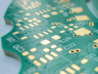
Printed Circuit Boards (PCBs) rely on vias to establish electrical connections between different layers. Vias are essential for high-density interconnect (HDI) designs, multilayer PCBs, and high-speed circuits. Understanding via requirements, manufacturing procedures, and different via types is crucial for PCB designers and engineers. This article explores PCB via specifications, fabrication processes, and common via classifications.
1. PCB Via Requirements
To ensure reliable PCB performance, vias must meet specific design and manufacturing requirements. Key considerations include:
1.1 Electrical Requirements
- Conductivity: Vias must provide low-resistance pathways for electrical signals.
- Current Carrying Capacity: Via size and plating thickness affect current handling.
- Impedance Control: High-speed signals require controlled impedance vias to minimize signal reflections.
1.2 Mechanical Requirements
- Aspect Ratio (Depth-to-Diameter Ratio): Standard PCBs typically support aspect ratios up to 8:1 (e.g., a 0.3mm via with a 2.4mm board thickness). Higher aspect ratios require specialized plating techniques.
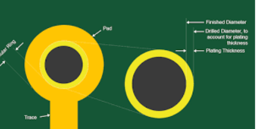
- Plating Thickness: Copper plating inside vias should be ≥ 25µm (1 mil) to ensure durability.
- Hole Wall Quality: Smooth via walls prevent plating voids and cracks.
1.3 Thermal Requirements
- Heat Dissipation: Thermal vias help transfer heat from components to other layers or heatsinks.
- Thermal Expansion: Vias must withstand thermal cycling without cracking.
1.4 Manufacturing & Assembly Constraints
- Minimum Via Size: Standard drill sizes range from 0.1mm to 0.3mm (laser-drilled microvias can be smaller).
- Registration Accuracy: Misalignment between layers can cause open or short circuits.
- Solder Masking: Some vias require tenting (covering with solder mask) to prevent solder wicking.
2. PCB Via Fabrication Procedures
The via manufacturing process involves several key steps:
2.1 Drilling
- Mechanical Drilling: Used for standard through-hole vias (≥ 0.2mm diameter).
- Laser Drilling: Required for microvias (< 0.1mm) in HDI PCBs.
2.2 Desmearing & Deburring
- Removes resin smear and debris from drilling to ensure proper plating adhesion.
2.3 Electroless Copper Deposition (Chemical Plating)
- A thin conductive layer is applied to the via walls to enable electroplating.
2.4 Electroplating
- Copper is electroplated to achieve the desired thickness (typically 25µm–50µm).
2.5 Via Filling (Optional)
- Conductive or non-conductive epoxy fills vias to improve reliability and solderability.
2.6 Via Capping (For Filled Vias)
- A copper cap is added to create a flat surface for component mounting.
2.7 Final Finishing
- Surface finishes like ENIG (Electroless Nickel Immersion Gold) or HASL (Hot Air Solder Leveling) are applied.
3. PCB Via Types
PCBs utilize different via types based on design requirements. The main classifications are:
3.1 Through-Hole Vias
- Description: Span the entire PCB thickness.
- Applications: Standard multilayer PCBs, high-power circuits.
- Advantages: Strong mechanical connection, good heat dissipation.
- Limitations: Occupies space on all layers, not suitable for HDI designs.
3.2 Blind Vias
- Description: Connect an outer layer to one or more inner layers but do not go through the entire board.
- Applications: High-density designs where space optimization is critical.
- Advantages: Saves space, improves signal integrity.
- Limitations: More expensive to manufacture due to laser drilling.
3.3 Buried Vias
- Description: Connect inner layers without reaching outer layers.
- Applications: Complex multilayer PCBs (e.g., smartphones, servers).
- Advantages: Maximizes routing space on outer layers.
- Limitations: Difficult to inspect and repair.
3.4 Microvias
- Description: Small vias (≤ 0.1mm) created with laser drilling.
- Types:
- Stacked Microvias: Multiple microvias stacked vertically.
- Staggered Microvias: Offset microvias to reduce stress.
- Applications: HDI PCBs, wearable electronics.
- Advantages: Enables ultra-high-density routing.
- Limitations: Requires advanced manufacturing techniques.
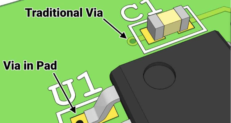
3.5 Via-in-Pad
- Description: Vias placed directly under component pads.
- Applications: BGA (Ball Grid Array) and fine-pitch components.
- Advantages: Saves space, improves signal performance.
- Limitations: Requires via filling to prevent solder wicking.
3.6 Thermal Vias
- Description: Used to transfer heat from components to other layers or heatsinks.
- Applications: Power electronics, LED PCBs.
- Advantages: Enhances thermal management.
- Limitations: May require additional copper pour for better heat dissipation.
4. Choosing the Right Via Type
Selecting the appropriate via depends on:
- Design Complexity: HDI designs need microvias, while standard PCBs use through-hole vias.
- Signal Speed: High-speed signals benefit from blind/buried vias to reduce stubs.
- Thermal Needs: Power circuits require thermal vias.
- Cost Constraints: Microvias and buried vias increase fabrication costs.
5. Conclusion
PCB vias are critical for multilayer interconnections, signal integrity, and thermal management. Designers must consider electrical, mechanical, and thermal requirements when selecting via types. Through-hole, blind, buried, and microvias each serve specific purposes, and the fabrication process must ensure proper plating and reliability. By understanding these factors, engineers can optimize PCB performance for various applications, from consumer electronics to aerospace systems.