How to Determine the Number of Layers in a PCB
Introduction
Printed Circuit Boards (PCBs) form the backbone of modern electronics, providing the physical platform for component mounting and electrical connections. As electronic devices become increasingly complex, the need for multilayer PCBs has grown substantially. Determining the number of layers in a PCB is essential for engineers, technicians, and procurement specialists for various reasons including design validation, quality control, reverse engineering, and cost estimation.
This comprehensive guide explores multiple methods to identify the layer count of a PCB, ranging from simple visual inspection to advanced analytical techniques. Understanding these methods enables professionals to make informed decisions about PCB specifications and verify manufacturer claims.
Visual Inspection Methods
1. Edge Examination
The most straightforward approach to estimate PCB layer count is by examining the board’s edge where the cross-section is visible:
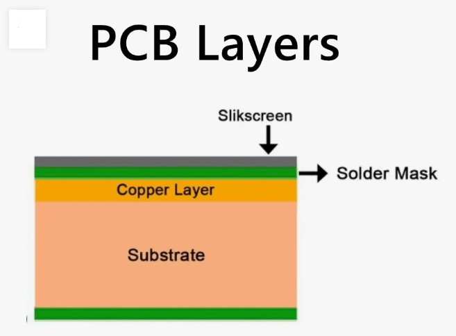
- Clean edge viewing: Hold the PCB at an angle to light to observe the layered structure
- Layer identification: Each conductive layer appears as a thin, shiny copper line separated by darker dielectric material
- Count technique: Count all visible copper layers, remembering that even inner layers may be visible at the edge
This method works best for boards with 4-16 layers where individual layers remain distinguishable. For very high layer counts (18+), layers may become too compressed for accurate visual counting.
2. Via Inspection
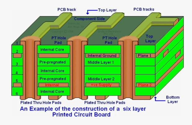
Examining vias (plated through-holes) provides additional clues about layer count:
- Through vias: Pass through all layers (not layer-count specific)
- Blind vias: Connect an outer layer to one or more inner layers without passing through the entire board
- Buried vias: Connect only inner layers without reaching either surface
The presence of blind and buried vias always indicates a multilayer PCB (typically 4+ layers), as these features don’t exist in single or double-sided boards.
3. Surface Features Analysis
Surface characteristics can suggest layer count:
- Component density: High-density designs typically require more layers
- Trace routing complexity: Dense, fine-pitch routing often necessitates additional layers
- Ground/power planes: Large copper areas may indicate dedicated power planes
While not definitive, these features correlate with layer count requirements in professional designs.
Physical Measurement Techniques
1. Thickness Measurement
PCB thickness relates to layer count:
- Standard layer thickness: Typically 0.1-0.2mm per layer pair (two conductive layers with dielectric)
- Total thickness estimation: Measure overall board thickness and divide by average layer pair thickness
- Calibration: Compare with known samples for better accuracy
This method provides only approximate results due to variations in dielectric materials and copper weights.
2. Microsection Analysis
Destructive testing provides definitive layer count:
- Sample preparation: Cut a small section from the PCB edge
- Polishing: Carefully polish the cross-section to a mirror finish
- Microscopy: Examine under optical or electron microscope to count layers
While highly accurate, this method damages the board and requires specialized equipment.
Non-Destructive Testing Methods
1. X-ray Inspection
X-ray systems reveal internal PCB structure:
- Transmission X-ray: Shows layer stacking and via connections
- Computed Tomography (CT): Creates 3D reconstructions of the PCB interior
- Layer differentiation: Different materials absorb X-rays differently, making layers distinguishable
X-ray provides detailed internal views without physical damage, though equipment costs can be prohibitive.
2. Terahertz Imaging
Emerging terahertz technology offers:
- Non-contact measurement: Safe for delicate components
- Layer resolution: Capable of distinguishing thin dielectric layers
- Material characterization: Identifies different dielectric materials
While promising, this technology remains primarily in research settings currently.
Electrical Testing Approaches
1. Capacitance Measurement
Layer count affects parasitic capacitance:
- Interlayer capacitance: Measured between surface traces and internal planes
- Reference data: Comparison with known designs helps estimate layers
- Limitations: Affected by many factors beyond just layer count
2. Time Domain Reflectometry (TDR)
TDR analyzes signal propagation:
- Transmission line analysis: Measures impedance variations corresponding to layer transitions
- Reflection patterns: Characteristic signatures indicate layer interfaces
- Equipment requirements: Needs high-frequency test gear
Design Documentation Review
When available, design files provide authoritative layer information:
- Gerber files: Layer count evident in file set
- PCB design software: Native files show exact stackup
- Manufacturing drawings: Often specify layer count explicitly
This method is only applicable when original design documentation is accessible.
Practical Considerations and Challenges
1. High-Density Interconnect (HDI) PCBs
HDI technologies complicate layer counting:
- Microvias: Extremely small vias may be difficult to detect
- Stacked vias: Multiple vias in vertical alignment
- Thin dielectrics: Reduced spacing between layers
2. Flexible and Rigid-Flex PCBs
These require special consideration:
- Variable thickness: Different areas may have different layer counts
- Flexible materials: May not exhibit clear layer boundaries
- 3D configurations: Folded sections complicate inspection
3. Board Age and Condition
Older or damaged PCBs present challenges:
- Edge oxidation: Can obscure layer boundaries
- Delamination: Separates layers, making counting difficult
- Contamination: Dirt or conformal coatings may hide features
Best Practices for Accurate Layer Counting
For reliable results:
- Combine multiple methods: Use both visual and technical approaches
- Use magnification: Microscopes enhance edge inspection
- Compare with known samples: Reference boards aid interpretation
- Consult manufacturers: When possible, obtain specifications
- Document findings: Record all observations and measurements
Conclusion
Determining the layer count of a PCB requires careful observation and often multiple complementary techniques. While simple visual methods suffice for many conventional boards, advanced technologies like X-ray imaging or microsection analysis may be necessary for complex or high-density designs. Understanding these various approaches enables electronics professionals to accurately assess PCB construction, verify specifications, and make informed decisions about board selection and application.
As PCB technology continues advancing with finer features and more sophisticated multilayer constructions, layer counting methodologies will likewise need to evolve. Future developments in non-destructive testing and automated image analysis promise to make this process more accurate and accessible across the electronics industry.