Step-by-Step Guide to Double-Sided PCB Reverse Engineering
Introduction
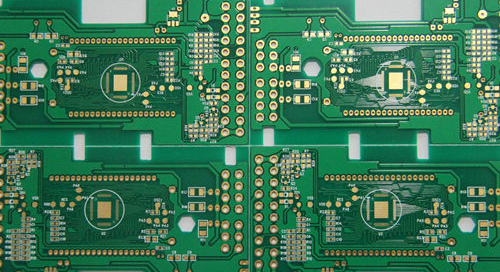
Reverse engineering a double-sided printed circuit board (PCB), commonly referred to as “PCB copying” or “cloning,” involves carefully analyzing and replicating an existing PCB design. This process is essential for repairing legacy systems, conducting competitive analysis, or reproducing obsolete boards when original documentation is unavailable.
This guide provides a detailed, step-by-step breakdown of the operations required to reverse-engineer a double-sided PCB accurately.
1. Preparation and Tools Required
Before starting, gather the necessary tools and materials:
- Digital camera or scanner (high resolution for capturing PCB details)
- Multimeter (for continuity testing)
- Soldering iron & desoldering tools (to remove components if needed)
- PCB design software (e.g., Altium Designer, KiCad, Eagle)
- Magnifying glass or microscope (for inspecting fine traces)
- Chemical etching solutions (if removing solder mask is necessary)
2. Documenting the Original PCB
Step 1: High-Resolution Imaging
- Take clear, well-lit photographs of both sides of the PCB.
- Ensure no shadows or reflections obscure traces or components.
- Use a scanner for flat PCBs to get precise images.
Step 2: Component Inventory
- List all components (resistors, capacitors, ICs, connectors, etc.).
- Note their values, part numbers, and orientations (polarity).
- Identify any proprietary or hard-to-find components.
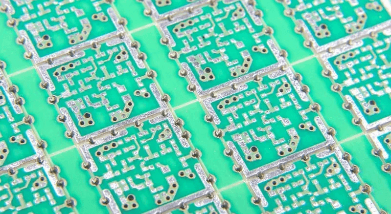
Step 3: Trace Mapping
- Visually track all copper traces on both sides.
- Use a multimeter in continuity mode to verify connections.
- Mark vias (holes connecting top and bottom layers).
3. Removing Components (If Necessary)
If the PCB must be stripped for better trace visibility:
- Desolder components carefully to avoid damaging pads.
- Group components by type and label them for reassembly.
- Clean the board to remove solder residue.
4. Creating the Schematic Diagram
Step 1: Drawing the Circuit Schematic
- Using PCB design software, recreate the circuit connections.
- Start with power and ground networks.
- Add ICs, passives, and connectors based on the component list.
Step 2: Verifying Connections
- Cross-check with the original PCB using continuity tests.
- Ensure all vias and jumpers are correctly mapped.
5. PCB Layout Design
Step 1: Setting Up the Design Software
- Define board dimensions based on the original PCB.
- Set layer properties (top and bottom copper layers).
Step 2: Placing Components
- Position components as per the original layout.
- Match footprints and pad sizes accurately.
Step 3: Routing Traces
- Manually route traces following the original PCB’s paths.
- Ensure trace widths match for power and signal lines.
- Replicate vias and through-hole connections.
Step 4: Adding Silkscreen and Solder Mask
- Mark component designators (R1, C2, U3, etc.).
- Apply solder mask openings where needed.
6. Design Verification
Step 1: Design Rule Check (DRC)
- Run DRC in the PCB software to detect errors.
- Verify spacing, trace widths, and via placements.
Step 2: Comparing with Original PCB
- Overlay the new design on scanned images for accuracy.
- Check for missing or incorrect connections.
7. Prototyping and Testing
Step 1: Manufacturing the Cloned PCB
- Export Gerber files and send them to a PCB fab house.
- Order a prototype for testing.
Step 2: Assembling the PCB
- Solder components onto the new board.
- Double-check orientations and placements.
Step 3: Functional Testing
- Power up the board and check for expected voltages.
- Test signal paths with an oscilloscope if necessary.
- Debug any issues by revisiting the schematic or layout.
8. Final Adjustments and Production
- If the prototype works, proceed with full-scale production.
- Document all changes for future reference.
Conclusion
Reverse engineering a double-sided PCB requires meticulous attention to detail, from initial documentation to final testing. By following these structured steps—imaging, component mapping, schematic recreation, layout design, and verification—you can accurately clone a PCB without original design files.
This process is invaluable for maintaining outdated electronics, conducting hardware analysis, or recreating proprietary designs legally. With the right tools and patience, even complex double-sided PCBs can be successfully reverse-engineered.