Root Cause Analysis and Prevention Strategies for PCB Blowholes
Abstract
Printed Circuit Board (PCB) blowholes, also known as plating voids or blow-outs, are critical defects that can compromise the reliability and functionality of electronic assemblies. These defects typically occur during the soldering process, where gas entrapment or improper plating leads to voids in plated through-holes (PTHs) or vias. This paper investigates the root causes of PCB blowholes, including material issues, process inconsistencies, and environmental factors. Additionally, effective prevention strategies are proposed to enhance PCB manufacturing quality and reliability.
1. Introduction
PCBs are essential components in modern electronics, providing mechanical support and electrical connections. However, defects such as blowholes can lead to intermittent connections, reduced current-carrying capacity, and eventual failure. Understanding the root causes and implementing preventive measures is crucial for improving yield and product longevity.
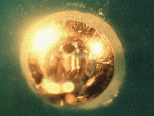
2. Definition and Types of PCB Blowholes
Blowholes are voids or gas pockets that form within or around plated through-holes (PTHs) or solder joints. They are categorized into:
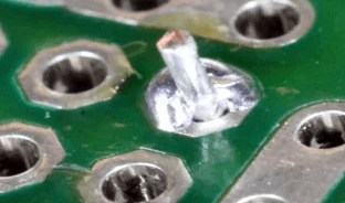
- Plating Voids: Gaps in the copper plating of PTHs due to poor electroplating.
- Solder Blowholes: Gas bubbles trapped in solder joints during reflow or wave soldering.
- Via Cracks: Fractures in vias due to thermal stress, leading to gas expansion.
3. Root Causes of PCB Blowholes
3.1 Material-Related Causes
- Poor Copper Plating Quality: Inadequate electroplating thickness or uneven deposition can create weak spots where gas accumulates.
- Substrate Moisture Absorption: Hygroscopic PCB materials (e.g., FR-4) absorb moisture, which vaporizes during soldering, causing blowholes.
- Contaminated Surface Finish: Oxidation or impurities on copper surfaces hinder proper solder wetting, increasing void formation.
3.2 Process-Related Causes
- Insufficient Drilling Quality: Rough or contaminated hole walls prevent uniform copper deposition.
- Improper Electroplating Parameters: Low current density or incorrect bath chemistry leads to thin or porous copper layers.
- Inadequate Pre-Baking: Failure to remove moisture before soldering results in steam-induced blowholes.
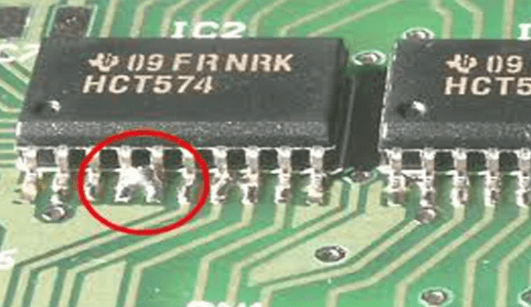
- Excessive Solder Temperature: Overheating causes rapid outgassing, trapping bubbles in solder joints.
3.3 Design-Related Causes
- Insufficient Via Aspect Ratio: High aspect ratio vias (depth/diameter) complicate plating, increasing void risks.
- Poor Thermal Relief Design: Uneven heat distribution during soldering leads to localized gas expansion.
4. Prevention Strategies
4.1 Material Selection and Handling
- Use High-Quality Substrates: Low-moisture-absorption materials (e.g., high-Tg FR-4) reduce outgassing.
- Ensure Proper Copper Plating: Implement strict thickness control (≥25µm for PTHs) and quality checks.
- Control Storage Conditions: Store PCBs in dry environments (<30% RH) and pre-bake (105-120°C for 2-4 hours) before assembly.
4.2 Process Optimization
- Improve Drilling and Desmearing: Use laser drilling or plasma desmearing for cleaner hole walls.
- Optimize Electroplating: Adjust current density, bath agitation, and chemical composition for uniform deposition.
- Reflow/Wave Soldering Control:
- Use nitrogen (N₂) atmosphere soldering to minimize oxidation.
- Apply proper temperature profiles (ramp-up rate: 1-3°C/sec, peak temp: 230-250°C).
4.3 Design Improvements
- Limit Via Aspect Ratio: Maintain aspect ratios < 8:1 for reliable plating.
- Implement Thermal Relief Pads: Reduce thermal stress on vias during soldering.
- Use Filled Vias: Conductive or non-conductive via fills prevent gas entrapment.
5. Inspection and Testing Methods
- Automated Optical Inspection (AOI): Detects surface-level voids.
- X-Ray Inspection: Identifies internal blowholes in PTHs and BGA joints.
- Cross-Sectional Analysis: Verifies plating integrity and void distribution.
6. Conclusion
PCB blowholes stem from material, process, and design deficiencies. By adopting stringent material controls, optimizing manufacturing processes, and improving PCB design, manufacturers can significantly reduce blowhole occurrences. Continuous monitoring through advanced inspection techniques ensures long-term reliability in electronic assemblies.