PCB Routing: Can Traces Be Run at Right Angles?
Introduction
Printed Circuit Board (PCB) design involves numerous considerations that affect the performance, reliability, and manufacturability of the final product. One of the long-standing debates in PCB layout concerns the use of right-angle (90-degree) bends in trace routing. Traditional wisdom in the electronics industry often warned against using right-angle traces, citing potential problems with signal integrity, manufacturing issues, and reliability concerns. However, with advancing technologies and changing design requirements, this conventional view has been challenged in recent years.
This article examines the validity of right-angle traces in modern PCB design by exploring the historical context, technical considerations, empirical evidence, and current industry practices regarding this controversial routing approach.
Historical Context of the Right-Angle Debate
The aversion to right-angle traces in PCB design dates back to the early days of the electronics industry. Several factors contributed to this longstanding design rule:
- Manufacturing Concerns: In the era of manual PCB design and less precise manufacturing processes, sharp right angles were believed to be problematic for etching. The concern was that acid traps could form in the internal corners, leading to over-etching and potential trace breakage.
- Signal Reflection Fears: As digital signals began operating at higher frequencies, engineers theorized that right-angle bends could cause impedance discontinuities that would lead to signal reflections.
- Electromagnetic Radiation: Some believed that sharp angles could act as point sources for electromagnetic interference (EMI) due to charge accumulation at the corners.
- Reliability Issues: There were concerns about mechanical stress concentration at sharp corners, particularly in flexible circuits or under thermal cycling conditions.
These concerns led to the widespread adoption of the 45-degree bend as the standard in PCB routing, with many design guidelines explicitly prohibiting right-angle traces.
Technical Analysis of Right-Angle Traces
To properly evaluate whether right-angle traces are acceptable in modern PCB design, we must examine the technical aspects from multiple perspectives:
Signal Integrity Considerations
At high frequencies, signal integrity becomes critical. The primary concerns with right-angle bends include:
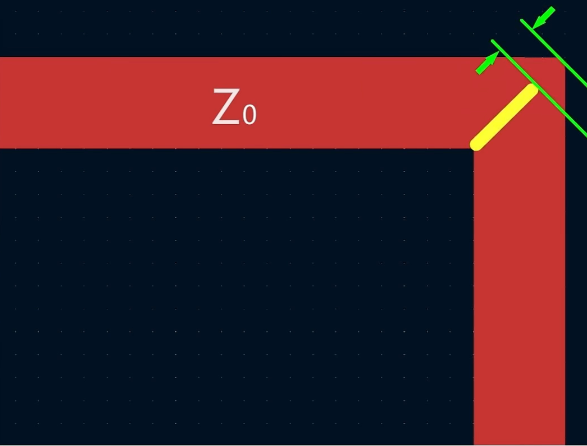
- Impedance Discontinuity: Any change in trace geometry affects its characteristic impedance. A right-angle bend effectively creates a slightly wider area at the corner (when viewed from above), which could cause a minor impedance variation.
- Capacitive Effects: The corner of a right-angle bend presents a small additional capacitance to the signal path. For very high-speed signals (typically above 10 GHz), this might become significant.
- Signal Reflection: The impedance discontinuity can cause signal reflections, leading to potential signal integrity issues like ringing or overshoot.
However, modern analysis shows that for most practical applications, the effects are negligible:
- The additional capacitance at a right-angle corner is typically in the range of femtofarads (10^-15 F)
- For signals below 1 GHz, the impact is generally insignificant
- The reflection caused by a single right-angle bend is often smaller than those caused by vias or connectors
Manufacturing Considerations
With modern PCB fabrication techniques:
- Photolithography Precision: Today’s manufacturing processes can reliably produce right-angle features without creating acid traps or etching problems.
- Minimum Feature Sizes: As trace widths have decreased, the relative impact of corner geometry has diminished.
- Design Rule Checks: Modern EDA tools can identify and prevent true manufacturing issues related to trace geometry.
EMI and Current Distribution
Early concerns about EMI radiation from right-angle corners have been largely disproven by empirical studies:
- Current Distribution: While theoretically current density might be slightly higher at the inside corner, the practical effect is minimal for typical PCB traces.
- Radiation Patterns: Measurements show no significant increase in EMI from boards with right-angle traces compared to those with 45-degree bends.
Empirical Evidence and Modern Practices
Recent studies and industry practices have challenged the traditional prohibition against right-angle routing:
- Experimental Measurements: Multiple controlled experiments have shown no measurable difference in signal integrity between 45-degree and 90-degree bends for signals below 10 GHz.
- Industry Adoption: Many major electronics companies now permit right-angle routing in their design guidelines, especially for digital circuits operating at common frequencies.
- High-Speed Design Experts: Prominent signal integrity engineers have published findings that right-angle bends are acceptable in most practical applications.
- Automated Routing Tools: Modern PCB autorouters often use right-angle patterns without compromising performance.
When Right-Angle Traces Might Still Be Problematic
While right-angle routing is generally acceptable in modern PCB design, there are specific cases where caution is warranted:
- Extremely High-Frequency Designs (above 10 GHz): The cumulative effect of many right-angle bends might become significant.
- RF and Microwave Circuits: Where impedance control is extremely critical, even minor discontinuities might need to be minimized.
- High-Power Applications: Where current density and thermal considerations are primary concerns.
- Flexible Circuits: Mechanical stress considerations might make rounded corners preferable.
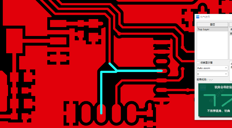
Best Practices for Right-Angle Routing
For designers considering right-angle traces, these practices can help ensure good results:
The Space Efficiency Advantage of Right-Angle Routing
One significant advantage of right-angle routing is improved space utilization:
- Higher Density Layouts: Right-angle traces can allow more compact routing in tight spaces.
- Reduced Layer Count: More efficient routing might enable designs with fewer layers.
- Simplified Routing: In some complex layouts, right-angle turns can simplify the routing process.
- Autorouter Efficiency: Right-angle patterns can improve autorouter performance in dense designs.
Psychological and Workflow Factors
The persistence of the right-angle prohibition may also relate to non-technical factors:
- Designer Psychology: The visual appearance of right-angle traces may subjectively seem “wrong” to experienced designers trained in the old guidelines.
- Corporate Design Rules: Many companies maintain conservative design rules that are slow to change, even when evidence supports updating them.
- Educational Inertia: Engineering curricula and textbooks often perpetuate traditional rules without critical re-examination.
Conclusion
The debate over right-angle PCB routing illustrates how engineering practices must evolve with technology. While the traditional prohibition against 90-degree traces was based on valid concerns for earlier manufacturing processes and lower-speed designs, modern evidence demonstrates that right-angle routing is generally acceptable for most contemporary PCB applications.
Designers should understand that:
- For the majority of digital designs (especially below 1 GHz), right-angle traces pose no significant problems.
- Modern PCB manufacturing can reliably produce right-angle features without quality issues.
- The signal integrity impact of a few right-angle bends is negligible compared to other common discontinuities like vias or connectors.
- Right-angle routing can offer tangible benefits in terms of board space utilization and routing efficiency.
However, as with all engineering decisions, context matters. While the blanket prohibition against right-angle traces is outdated, designers should still apply judgment based on their specific requirements, particularly for very high-frequency, RF, or specialized applications. The most informed approach is to understand the underlying physics and make routing decisions based on actual design requirements rather than adhering to outdated rules of thumb.
As PCB technology continues to advance with higher densities and faster signals, the industry’s understanding of optimal routing practices will continue to evolve. The key is to base design decisions on empirical evidence and current manufacturing capabilities rather than unquestioned tradition.