Methods for Adding Process Edges and Fiducial Marks in PCB Design
Introduction to PCB Manufacturing Aids
Printed Circuit Board (PCB) design involves not only the layout of electrical connections but also the incorporation of manufacturing aids that facilitate efficient and accurate production. Two critical elements in this category are process edges (also called manufacturing edges or breakaway tabs) and fiducial marks (often called mark points). These features play vital roles in the PCB fabrication and assembly processes, ensuring proper handling during manufacturing and precise component placement during assembly.
This article provides a comprehensive guide to implementing process edges and fiducial marks in PCB designs, covering their purposes, design requirements, placement strategies, and implementation methods across various design tools.
Understanding Process Edges in PCB Design
Definition and Purpose of Process Edges
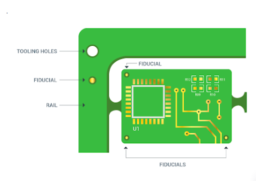
Process edges, sometimes referred to as manufacturing margins or breakaway tabs, are additional border areas added to PCBs that extend beyond the actual circuit area. These edges serve several important functions:
- Machine Handling: Provides space for conveyor belts and clamping mechanisms in automated equipment
- Panelization Support: Allows for proper spacing when multiple PCBs are arrayed in a panel
- Process Stability: Maintains consistent material dimensions through various manufacturing steps
- Breakaway Convenience: Enables clean separation of individual boards after processing
Design Specifications for Process Edges
When adding process edges to your PCB design, consider these technical specifications:
- Typical Width: 5-10mm (0.2-0.4 inches) per side, depending on equipment requirements
- Minimum Width: 3mm (0.12 inches) for basic handling
- Material Continuity: Must maintain the same base material as the main PCB
- Tooling Holes: Often include mounting holes in the process edges for fixture alignment
- Breakaway Methods: May include V-grooves, perforated tabs, or mouse bites for separation
Implementation Methods for Process Edges
1. Manual Outline Extension in CAD Tools
Most PCB design software allows direct modification of the board outline:
- In Altium Designer: Use “Design » Board Shape » Redefine Board Shape”
- In KiCad: Modify the edge cuts layer graphics
- In Cadence Allegro: Use “Outline Edit” mode
2. Panelization Tools
Many CAD packages include panelization features that automatically add process edges:
- Altium’s “PCB Panelization” tool
- KiCad’s “Board Array” feature with margins
- Mentor’s “Panel Editor”
3. Scripting/Automation
For complex or repetitive requirements, scripts can automate edge addition:
- Use Python scripts with PCB design APIs
- Implement custom ULPs in EAGLE
- Create Skill scripts for Allegro
4. Manufacturing Notes
When process edges are added by the fabricator:
- Clearly specify requirements in fabrication drawings
- Include detailed notes in Gerber files
- Communicate with your manufacturer about specific needs
Fiducial Marks in PCB Design
Fundamentals of Fiducial Marks
Fiducial marks (or fiducials) are reference points used by automated assembly equipment to accurately position components on a PCB. These marks provide:
- Global Positioning: Reference for the entire board’s position
- Local Alignment: Precise positioning for fine-pitch components
- Orientation Reference: Determination of board rotation
- Scale Calibration: Compensation for material expansion/contraction
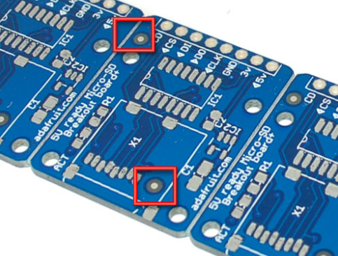
Types of Fiducial Marks
1. Global Fiducials
- Typically 3 marks placed on board corners or process edges
- Used for overall board alignment
- Required for all SMT assemblies
2. Local Fiducials
- Placed near high-density or precision components (BGAs, QFNs, etc.)
- Usually 2 marks per component area
- Provides enhanced placement accuracy
3. Panel Fiducials
- Located on process edges of panelized boards
- Used for panel-level alignment
Design Requirements for Fiducial Marks
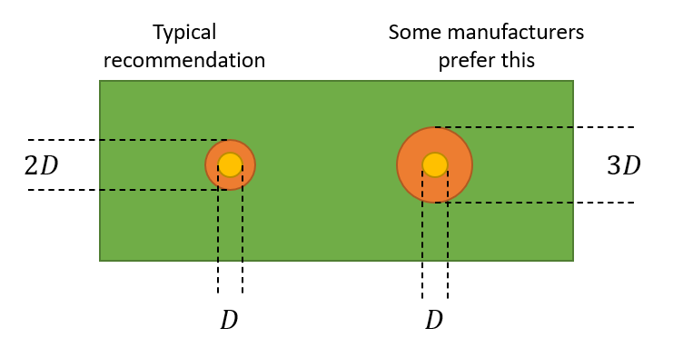
Shape and Size:
- Standard: 1mm (0.04″) diameter solid copper circles
- Minimum: 0.5mm diameter
- Maximum: 3mm diameter
- Non-standard shapes (crosses, diamonds) may be used but require verification
Clearance:
- 2mm minimum clearance around the mark (no copper, solder mask, or silkscreen)
- 3mm preferred for machine vision reliability
Layer Composition:
- Top/bottom copper layer (usually same as components being placed)
- Exposed copper (no solder mask) is most common
- Alternatively, may use solder mask-defined marks
Placement Rules:
- Global fiducials: 3 marks asymmetrically placed (to determine orientation)
- Local fiducials: 2 marks diagonally opposite near component
- Minimum distance from board edge: 5mm (including clearance)
Implementing Fiducial Marks in PCB Designs
1. Manual Placement in CAD Tools
Most PCB design software includes fiducial mark libraries or creation tools:
- Altium Designer:
- Use “Place » Fiducial” from menus
- Available in PCB Libraries panel
- Customizable through PCB Library editor
- KiCad:
- Create as custom footprints
- Add to board as components
- Available in community libraries
- Cadence Allegro:
- Use “Manufacturing » Fiducial” option
- Create symbols in symbol editor
2. Automated Placement Tools
Some advanced tools offer automated fiducial placement:
- Design rule-driven placement
- Panelization tools with automatic fiducial addition
- Script-based placement for large designs
3. Library Components
Many CAD systems include standard fiducial mark components:
- IPC-7351 compliant footprints
- Customizable size and clearance parameters
- Multiple layer options (top, bottom, both)
4. Verification Methods
After placement, verify:
- Clearance zones around marks
- Asymmetric placement for orientation
- Appropriate quantity for board complexity
- Consistency with manufacturer capabilities
Combined Implementation Strategies
Process Edge and Fiducial Integration
For optimal manufacturability, process edges and fiducial marks should be designed as an integrated system:
- Place Global Fiducials on Process Edges:
- Allows use before board separation
- Provides reference for depaneling equipment
- Include Tooling Holes in Process Edges:
- Aligns with fiducial marks for consistent reference
- Combined with fiducials for multi-stage processes
- Consider Breakaway Impact:
- Ensure fiducials remain until needed
- Avoid placing critical marks near separation lines
Design for Manufacturing (DFM) Considerations
When implementing these features:
- Consult Manufacturer Guidelines:
- Obtain specific requirements from your fabrication partner
- Verify machine capabilities and limitations
- Standardize Across Designs:
- Create templates with pre-defined edges and marks
- Develop company-specific design rules
- Document Clearly:
- Include in fabrication drawings
- Note special requirements explicitly
- Provide layer-by-layer specifications
Advanced Techniques
For complex or high-volume production:
- Dual-Purpose Features:
- Use tooling holes as visual fiducials
- Incorporate test points near fiducials
- Multi-Stage Fiducials:
- Different marks for fabrication vs. assembly
- Color-contrasted marks for various processes
- Dynamic Clearance Zones:
- Adjust clearances based on mark size
- Implement tear-drop clearances for high-reliability
Software-Specific Implementation Guides
Altium Designer Methods
Adding Process Edges:
- Open PCB document
- Select “Design » Board Shape » Redefine Board Shape”
- Draw new outline extending beyond circuit area
- Add tooling holes in extended areas
Creating Fiducial Marks:
- Access “Place » Fiducial” from menus
- Configure properties in Properties panel:
- Layer: Top/Bottom
- Size: 1mm diameter
- Clearance: 2mm
- Place in triangular pattern for global marks
KiCad Implementation
Process Edge Addition:
- Edit “Edge.Cuts” layer graphics
- Use line tools to extend board outline
- Add separate outline for breakaway tabs
Fiducial Mark Creation:
- Create or import fiducial footprint:
- Copper pad with appropriate size
- Courtyard area for clearance
- Place as standard component
- Verify clearance in DRC check
Cadence Allegro Techniques
Process Edge Setup:
- Use “Outline Editor” mode
- Create additional outline segments
- Specify as manufacturing border
Fiducial Implementation:
- Select “Manufacturing » Fiducial”
- Choose from library or create new
- Place with appropriate spacing
- Run DRC for clearance verification
Common Mistakes and Troubleshooting
Process Edge Pitfalls
- Insufficient Width:
- Symptom: Handling issues during fabrication
- Solution: Verify minimum requirements with manufacturer
- Improper Breakaway Design:
- Symptom: Rough edges or board damage
- Solution: Implement proper V-groove or tab design
- Missing Tooling Holes:
- Symptom: Misalignment in processing
- Solution: Add standard tooling holes in edges
Fiducial Mark Errors
- Inadequate Clearance:
- Symptom: Machine vision recognition failures
- Solution: Ensure proper clearance zones
- Symmetrical Placement:
- Symptom: Orientation detection problems
- Solution: Use asymmetric three-point placement
- Inconsistent Layers:
- Symptom: Marks not visible to assembly equipment
- Solution: Verify mark presence on correct layers
Conclusion and Best Practices
Effective implementation of process edges and fiducial marks significantly enhances PCB manufacturability and assembly accuracy. By following these guidelines:
- Standardize Early: Establish company-wide standards for these features
- Communicate with Manufacturers: Validate requirements before finalizing designs
- Use CAD Tools Effectively: Leverage automation and library features
- Verify Thoroughly: Run DRC checks specifically for manufacturing features
- Document Completely: Include all specifications in fabrication packages
Properly designed process edges and fiducial marks reduce manufacturing errors, improve yields, and ultimately contribute to higher quality electronic products. As PCB technology advances with finer pitches and higher densities, these manufacturing aids become even more critical for successful production.
Remember that while general guidelines exist, always consult with your specific fabrication and assembly partners for their exact requirements, as equipment capabilities vary between manufacturers. By incorporating these features thoughtfully during the design phase, you can avoid costly revisions and delays in your PCB manufacturing process.