How to Judge the Quality of a PCB Circuit Board: A Comprehensive Guide
Printed Circuit Boards (PCBs) form the backbone of modern electronics, serving as the physical platform that connects and supports various electronic components. As electronic devices become increasingly sophisticated, the quality of PCBs has never been more critical to product performance and reliability. This 2000-word guide provides a thorough examination of how to assess PCB quality through visual inspection, physical testing, electrical verification, and advanced analysis techniques.
I. Introduction to PCB Quality Assessment
The evaluation of PCB quality encompasses multiple dimensions, from basic visual checks to sophisticated electrical and functional tests. A high-quality PCB should meet all design specifications, demonstrate reliable electrical performance, and maintain structural integrity throughout its intended lifespan. Understanding how to properly assess PCB quality is essential for engineers, technicians, and quality control professionals working with electronic products.
II. Visual Inspection: The First Line of Quality Defense
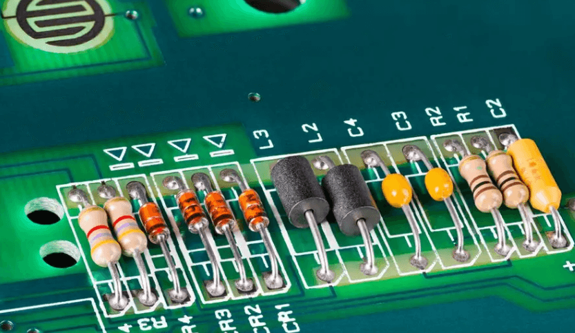
1. Surface Quality Examination
Begin by examining the PCB surface under proper lighting conditions (preferably white light at 500-1000 lux). Look for:
- Solder mask application: Should be even, without bubbles, peeling, or uneven coverage
- Silkscreen quality: Legible text and markings that are properly aligned
- Surface contaminants: Absence of flux residues, fingerprints, or foreign particles
- Discoloration: Uniform color without unusual spots or streaks
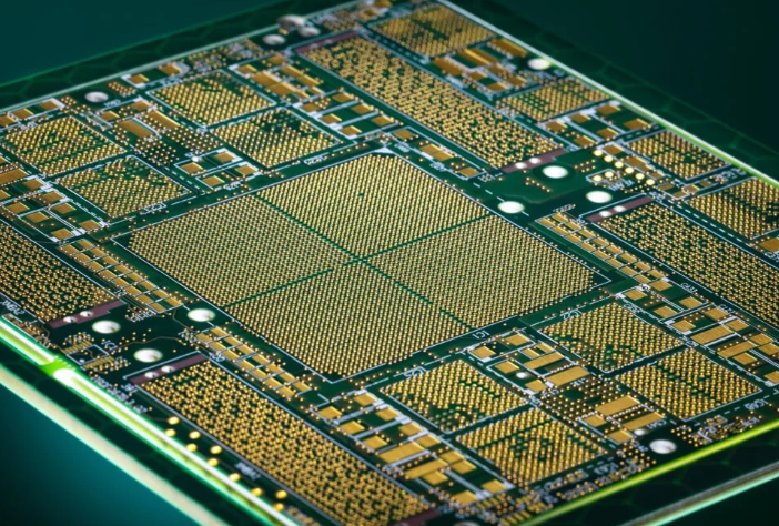
2. Copper Trace Inspection
Use magnification (3-10x) to examine copper traces:
- Trace width consistency: Should match design specifications without narrowing
- Edge smoothness: Clean, well-defined edges without roughness or “mouse bites”
- Copper thickness: Verify through cross-section if possible; should meet specified oz/ft² requirements
3. Solder Pad Evaluation
Assess solder pads for:
- Proper size and shape: According to design files
- Surface finish: Consistent plating (HASL, ENIG, OSP, etc.) without oxidation
- Registration: Perfect alignment with drilled holes
4. Hole Quality Assessment
Examine drilled and plated through-holes:
- Plating quality: Complete barrel coverage without voids or cracks
- Hole wall smoothness: Uniform interior surface
- Registration: Centered in pads without breakout
III. Physical and Dimensional Verification
1. Dimensional Accuracy
Measure critical dimensions using precision calipers or optical measurement systems:
- Board outline: Verify against design specifications
- Hole sizes and positions: Confirm diameter and positional accuracy
- Component placement: Check alignment with CAD data
2. Material Quality
Evaluate PCB substrate:
- Laminate material: Verify correct type (FR-4, high-frequency, etc.)
- Thickness uniformity: Measure at multiple points
- Delamination: Check for layer separation using cross-polarized light
3. Mechanical Strength Testing
Perform tests to verify structural integrity:
- Peel strength: Measure copper adhesion (typically >1N/mm)
- Flexural strength: Especially important for flexible PCBs
- Thermal stress resistance: Assess via thermal cycling tests

IV. Electrical Testing and Performance Verification
1. Continuity Testing
Use a multimeter or dedicated continuity tester to:
- Verify all intended connections
- Check for unintended shorts between nets
- Test via reliability
2. Insulation Resistance Measurement
Measure resistance between isolated conductors:
- Typical requirements: >100MΩ at 100VDC
- Perform after humidity exposure if applicable
3. High Voltage Testing
Apply elevated voltage (typically 500V-1500V) to verify:
- Dielectric strength
- Clearance and creepage adequacy
4. Impedance Verification
For high-speed designs:
- Measure characteristic impedance of controlled impedance traces
- Verify matching to design values (typically ±10% tolerance)
V. Advanced Testing Methods
1. Automated Optical Inspection (AOI)
Machine vision systems can:
- Detect surface defects with high precision
- Verify component placement accuracy
- Identify soldering issues
2. X-ray Inspection
Essential for examining:
- Hidden solder joints (BGA, QFN components)
- Internal layer connections
- Via fill quality
3. Flying Probe Testing
Provides comprehensive electrical verification:
- Checks opens and shorts
- Measures component values
- Verifies net connectivity
4. Functional Testing
System-level verification:
- Power-up tests
- Signal integrity measurements
- Full operational verification
VI. Environmental and Reliability Testing
1. Thermal Stress Testing
Subject PCBs to:
- Thermal cycling (-40°C to +125°C typical)
- Thermal shock tests
- High-temperature operation
2. Humidity Testing
Evaluate performance under:
- Damp heat (85°C/85% RH)
- Temperature-humidity bias
- Moisture sensitivity levels
3. Vibration and Mechanical Shock
Verify robustness against:
- Transportation stresses
- Operational vibration
- Mechanical impacts
VII. Assessing Manufacturing Process Quality
1. Process Control Verification
Review manufacturer’s:
- Process control charts
- Statistical process control data
- Yield reports
2. Material Certifications
Verify:
- Laminate certifications
- Copper foil specifications
- Surface finish documentation
3. Quality Management Systems
Check for:
- ISO 9001 certification
- IPC compliance
- Industry-specific qualifications
VIII. Industry Standards for PCB Quality
Familiarize yourself with key standards:
- IPC-A-600: Acceptability of Printed Boards
- IPC-6012: Qualification and Performance Specification for Rigid PCBs
- IPC-A-610: Acceptability of Electronic Assemblies
- IEC 61189: Test methods for electrical materials
IX. Common PCB Defects and Their Implications
Learn to recognize and evaluate:
- Open circuits: Broken traces or poor plating
- Shorts: Solder bridges or copper whiskers
- Plating voids: Incomplete hole barrel plating
- Delamination: Layer separation
- Warpage: Excessive board bending
X. Conclusion: Comprehensive Quality Assessment
Judging PCB quality requires a multifaceted approach combining visual inspection, physical measurements, electrical testing, and reliability verification. By systematically applying these evaluation methods and comparing results against design specifications and industry standards, you can accurately determine PCB quality and identify potential issues before they affect product performance.
Remember that PCB quality assessment isn’t merely about pass/fail determinations—it’s about understanding how various quality factors impact the reliability and longevity of the final product. Developing expertise in comprehensive PCB evaluation will significantly contribute to the success of your electronic products and projects.
By implementing thorough quality assessment protocols, manufacturers and users can ensure that PCBs meet the demanding requirements of today’s electronic applications, from consumer devices to mission-critical systems. The investment in proper PCB evaluation pays dividends through improved product reliability, reduced field failures, and enhanced customer satisfaction.