LED Packaging: A Comprehensive Overview
Introduction
Light Emitting Diodes (LEDs) have revolutionized the lighting industry with their energy efficiency, long lifespan, and versatility in applications ranging from general illumination to specialized uses in displays, automotive lighting, and medical devices. The performance and reliability of LEDs are heavily dependent on their packaging structure and technology. LED packaging serves multiple critical functions: it protects the delicate semiconductor die, provides electrical connections, manages heat dissipation, and often shapes the light output. This article provides a detailed examination of LED packaging structures, materials, and the latest technological advancements in this field.
1. Fundamental Structure of LED Packages
1.1 Basic Components
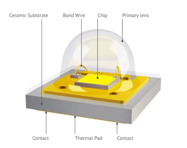
A typical LED package consists of several key components:
- LED Chip (Die): The semiconductor device that emits light when current flows through it. The chip is typically made from III-V compound semiconductors like GaN (for blue/white LEDs) or AlInGaP (for red/yellow LEDs).
- Substrate/Lead Frame: Provides mechanical support and electrical connections to the chip. Common materials include copper, aluminum, ceramics, or specialized plastic composites.
- Bonding Wires: Typically gold or copper wires that connect the chip electrically to the package leads.
- Encapsulant: A transparent material (often silicone or epoxy) that protects the chip and may include phosphors for wavelength conversion in white LEDs.
- Heat Sink: For high-power LEDs, an additional thermal management component is often integrated into the package.
1.2 Electrical Connections
LED packages must provide reliable electrical connections while maintaining electrical isolation where needed. The two main connection methods are:
- Wire Bonding: Traditional method using thin gold or copper wires to connect the chip to the leads.
- Flip-Chip: The chip is mounted upside-down with solder bumps providing both electrical connection and thermal path, eliminating the need for wire bonds.
2. Common LED Package Types
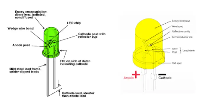
2.1 Through-Hole Packages
- Lamp LEDs (5mm, 3mm): The traditional LED package with a molded plastic body and two leads for through-hole PCB mounting. The epoxy lens shapes the light output.
- Super Flux (Piranha): Four-lead packages offering better heat dissipation than standard lamp LEDs, often used in automotive applications.
2.2 Surface Mount Device (SMD) Packages
- PLCC (Plastic Leaded Chip Carrier): Common low-to-medium power packages (e.g., 3528, 5050) with a plastic body and reflective cup to enhance light extraction.
- High-Power SMDs: Larger packages (e.g., 5630, 3030) designed to handle higher currents with improved thermal paths.
- Chip-Scale Packages (CSP): Nearly chip-sized packages that eliminate traditional lead frames, offering better thermal performance and higher density.
2.3 High-Power Packages
- Ceramic Packages: Use alumina or aluminum nitride substrates for superior thermal performance in high-brightness applications.
- COB (Chip-on-Board): Multiple LED chips mounted directly on a substrate (often ceramic or metal-core PCB) and covered with a single phosphor layer, creating an extended light source.
- Multi-Chip Packages: Integrate several LED chips in one package for higher lumen output or color mixing capabilities.
3. Advanced Packaging Technologies
3.1 Flip-Chip Technology
Flip-chip mounting offers several advantages over traditional wire bonding:
- Better thermal performance as heat can conduct directly through the solder bumps
- Higher reliability by eliminating wire bonds that can fail due to thermal cycling
- Smaller package size and better current spreading
- Improved high-frequency performance for communication LEDs
3.2 Wafer-Level Packaging (WLP)
WLP processes perform packaging steps at the wafer level before dicing, offering:
- Significant size reduction (true chip-scale packages)
- Batch processing for cost reduction
- Improved thermal and electrical performance
- Better mechanical robustness
3.3 Remote Phosphor Technology
Instead of applying phosphor directly on the chip, remote phosphor separates the conversion layer:
- Reduces heat stress on phosphor materials
- Enables better color uniformity
- Allows independent optimization of LED and phosphor components
- Provides design flexibility in light mixing
3.4 Advanced Thermal Management
As LED power densities increase, innovative thermal solutions have emerged:
- Direct Copper Bonding (DCB): Copper layers bonded to ceramic substrates for excellent thermal conductivity with electrical isolation.
- Vapor Chambers: Two-phase cooling systems integrated into LED packages for ultra-high-power applications.
- Thermally Conductive Plastics: Advanced polymer composites that combine electrical insulation with good thermal performance.
- Microfluidic Cooling: Emerging technology using tiny fluid channels for active cooling in extreme applications.
4. Materials in LED Packaging
4.1 Encapsulation Materials
- Epoxy Resins: Traditional material with good mechanical properties but prone to yellowing under high temperature/UV exposure.
- Silicones: Higher thermal and UV stability than epoxies, now widely used in high-power and long-life applications.
- Glass: Emerging material for extreme environments, offering perfect UV stability and hermetic sealing.
4.2 Substrate Materials
- FR4: Standard PCB material for low-power LEDs, limited by thermal conductivity.
- Metal Core PCBs (MCPCB): Aluminum or copper substrates with dielectric layers for better heat spreading.
- Ceramics (Al2O3, AlN, BeO): Excellent thermal and electrical properties for high-performance packages.
- Composite Substrates: Materials like copper-molybdenum or copper-diamond for specialized applications.
4.3 Phosphor Materials
- YAG:Ce: Yellow phosphor commonly used in blue-pumped white LEDs.
- Nitride and Oxynitride Phosphors: Red and green phosphors with better thermal stability.
- Quantum Dots: Nanocrystals offering narrow emission bands for wide color gamut displays.
- Phosphor-in-Glass (PiG): Durable alternative to traditional phosphor-in-silicone for harsh environments.
5. Optical Design in LED Packaging
5.1 Light Extraction Enhancement
- Surface texturing of chips and encapsulants
- Reflective sidewalls and cups
- High refractive index encapsulants
- Patterned phosphor layers for improved conversion efficiency
5.2 Beam Shaping
- Primary optics (lenses integrated in the package)
- Secondary optics (external reflectors or lenses)
- Freeform optics for precise light distribution
- Micro-lens arrays for uniform illumination
5.3 Color Mixing
- Multi-chip packages with different color LEDs
- Phosphor layer design for uniform color temperature
- Wavelength-converting materials arrangement
- Hybrid approaches combining direct and converted emission
6. Reliability Considerations
6.1 Failure Mechanisms
- Thermal stress causing delamination or cracking
- Moisture ingress leading to corrosion
- Phosphor thermal degradation
- Solder joint fatigue
- Electrochemical migration
6.2 Reliability Testing
- Temperature cycling tests
- Damp heat testing
- High-temperature operating life (HTOL)
- Photometric maintenance testing (LM-80)
- Mechanical shock and vibration tests
6.3 Design for Reliability
- CTE matching between materials
- Robust moisture barriers
- Stress-relief features in package design
- Proper thermal path design
- Accelerated life testing protocols
7. Emerging Trends in LED Packaging
7.1 Mini and Micro LEDs
- Mini-LEDs (100-200μm) for high-end displays
- Micro-LEDs (<100μm) for next-generation displays
- Mass transfer challenges and solutions
- Color conversion approaches for micro-LEDs
7.2 UV LED Packaging
- Specialized materials for UV transparency
- Hermetic sealing against environmental degradation
- Thermal management for high-power UV applications
- Safety considerations in package design
7.3 Smart and Integrated LED Packages
- Packages with integrated drivers or control circuitry
- Color-tunable multi-chip packages
- Packages with built-in sensors (temperature, light)
- IoT-enabled LED packages with communication capabilities
7.4 Sustainable Packaging
- Lead-free and RoHS compliant materials
- Recyclable package designs
- Reduced material usage through advanced designs
- Longer-life packages to reduce replacement frequency
Conclusion
LED packaging technology has evolved dramatically from simple lamp-style packages to sophisticated systems integrating advanced thermal management, optical control, and sometimes even electronics. The choice of package structure significantly impacts the LED’s performance, reliability, and suitability for specific applications. As LED technology continues to advance, packaging innovations will play a crucial role in enabling higher efficiencies, greater reliability, and new functionalities. Future developments in materials, manufacturing processes, and design approaches will further push the boundaries of what’s possible with solid-state lighting, opening up new applications and improving performance across all sectors of the lighting industry.