Multilayer PCB Structure Analysis: A Comprehensive Guide
Introduction
Printed Circuit Boards (PCBs) are the backbone of modern electronics, providing mechanical support and electrical connectivity for electronic components. As technology advances, the demand for compact, high-performance devices has led to the widespread adoption of multilayer PCBs. These boards consist of multiple layers of conductive and insulating materials, enabling complex circuit designs in a limited space.
This article provides an in-depth analysis of the structure of multilayer PCBs, covering their composition, layer arrangement, materials, manufacturing processes, and key advantages.
1. What is a Multilayer PCB?
A multilayer PCB is a circuit board with three or more conductive copper layers laminated together with insulating (dielectric) materials. These layers are interconnected through vias (plated-through holes), allowing signals and power to travel between different layers.
Key Characteristics:
- High circuit density – More routing options in a compact space.
- Improved signal integrity – Reduced electromagnetic interference (EMI) and crosstalk.
- Enhanced thermal management – Better heat dissipation through internal ground/power planes.
- Higher reliability – Suitable for complex and high-speed applications.
2. Multilayer PCB Structure Breakdown
A typical multilayer PCB consists of the following structural components:
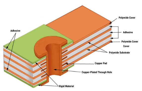
2.1. Core Layer
- The core is the central substrate, usually made of FR-4 (Flame Retardant-4), a fiberglass-reinforced epoxy laminate.
- It provides mechanical rigidity and houses the first copper layers (inner layers).
2.2. Prepreg (Pre-Impregnated) Layers
- Prepreg is a partially cured dielectric material (e.g., fiberglass soaked in resin) that bonds the core and copper layers.
- When heated and pressed during lamination, it fully cures, forming a solid insulating layer.
2.3. Copper Foil Layers
- Thin sheets of electrolytic copper foil (typically 0.5 oz to 2 oz in thickness) are laminated onto prepreg layers.
- These foils are etched to form conductive traces, pads, and planes.
2.4. Inner Layer Circuitry
- Inner layers contain signal traces, power planes, and ground planes.
- These are etched before lamination and are crucial for high-speed signal routing.
2.5. Outer Layers (Top & Bottom)
- The outermost layers consist of solder mask, silkscreen, and exposed copper pads for component mounting.
- These layers are typically used for component placement and external connections.
2.6. Solder Mask
- A protective polymer coating (usually green, but other colors are available) applied over copper traces to prevent oxidation and short circuits.
2.7. Silkscreen (Legend)
- White (or colored) markings indicating component placement, polarity, and reference designators.
2.8. Vias (Interlayer Connections)
- Through-hole vias – Pass through all layers.
- Blind vias – Connect an outer layer to an inner layer.
- Buried vias – Connect only inner layers (not visible from the surface).

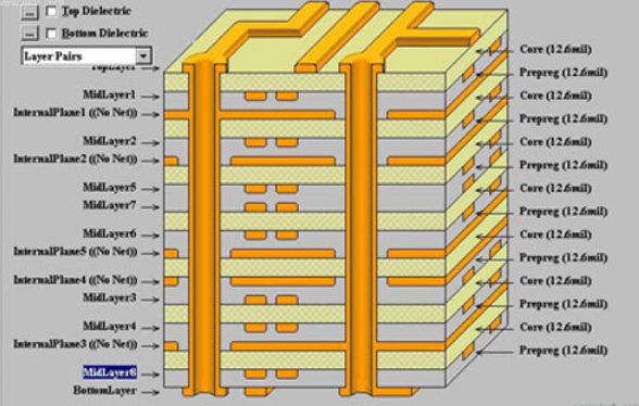
3. Layer Stackup Configuration
The arrangement of layers in a multilayer PCB is called the stackup. A well-designed stackup ensures signal integrity, reduces EMI, and improves power distribution.
Common Stackup Examples:
4-Layer PCB:
- Top Layer (Signal)
- Ground Plane (Inner Layer 1)
- Power Plane (Inner Layer 2)
- Bottom Layer (Signal)
6-Layer PCB:
- Top Layer (Signal)
- Ground Plane (Inner Layer 1)
- Signal Layer (Inner Layer 2)
- Power Plane (Inner Layer 3)
- Signal Layer (Inner Layer 4)
- Bottom Layer (Signal)
8-Layer PCB (High-Speed Design):
- Top Layer (Signal)
- Ground Plane
- Signal Layer (High-Speed)
- Power Plane
- Ground Plane
- Signal Layer (High-Speed)
- Power Plane
- Bottom Layer (Signal)
Key Considerations for Stackup Design:
- Symmetry – Prevents warping during manufacturing.
- Signal Layer Adjacency to Planes – Reduces EMI and crosstalk.
- Controlled Impedance – Critical for high-frequency signals.
4. Materials Used in Multilayer PCBs
4.1. Substrate Materials
- FR-4 – Most common, cost-effective, good mechanical strength.
- High-Tg FR-4 – Better thermal resistance for high-power applications.
- Polyimide – High-temperature and flexible PCBs.
- Rogers Material – Low-loss dielectric for RF/microwave circuits.
4.2. Copper Foil
- Electrodeposited (ED) Copper – Standard for most PCBs.
- Rolled Annealed (RA) Copper – Better flexibility for high-frequency designs.
4.3. Prepreg Types
- Standard FR-4 Prepreg
- High-Speed Low-Loss Prepreg (e.g., Megtron 6, Isola 370HR)
5. Manufacturing Process of Multilayer PCBs
Step 1: Inner Layer Fabrication
- Copper-clad laminates are cleaned.
- Photoresist is applied, exposed to UV light through a photomask, and developed.
- Etching removes unwanted copper, leaving circuit traces.
Step 2: Oxide Treatment & Lamination
- Inner layers are treated with oxide to improve adhesion.
- Layers are stacked with prepreg and pressed under high temperature.
Step 3: Drilling & Plating
- Holes are drilled for vias and component leads.
- Electroless copper plating creates conductive pathways.
Step 4: Outer Layer Patterning
- Similar to inner layers but involves additional plating (electroplating).
Step 5: Solder Mask & Silkscreen Application
- Liquid photoimageable solder mask (LPSM) is applied and cured.
- Silkscreen markings are printed.
Step 6: Surface Finish
- HASL (Hot Air Solder Leveling)
- ENIG (Electroless Nickel Immersion Gold)
- OSP (Organic Solderability Preservative)
Step 7: Electrical Testing & Inspection
- Automated Optical Inspection (AOI)
- Flying Probe Testing
- Impedance Testing (for high-speed designs)
6. Advantages of Multilayer PCBs
- Higher Component Density – More circuits in a smaller footprint.
- Better Signal Performance – Reduced noise and crosstalk.
- Improved Power Distribution – Dedicated power and ground planes.
- Enhanced Durability – Stronger than single/double-layer boards.
- Thermal Management – Heat dissipation through internal planes.
7. Applications of Multilayer PCBs
- Consumer Electronics (Smartphones, Laptops)
- Telecommunications (5G, Routers)
- Automotive Electronics (ECUs, ADAS)
- Medical Devices (MRI Machines, Pacemakers)
- Aerospace & Defense (Avionics, Radar Systems)
8. Conclusion
Multilayer PCBs are essential for modern high-performance electronics, offering superior signal integrity, power distribution, and space efficiency. Understanding their structure, materials, and manufacturing processes helps engineers design more reliable and efficient PCBs for advanced applications.
As technology evolves, multilayer PCBs will continue to push the boundaries of miniaturization and high-speed performance, making them indispensable in next-generation electronic devices.