High-Difficulty Printed Circuit Boards: Design, Manufacturing, and Applications
Introduction to High-Difficulty PCBs
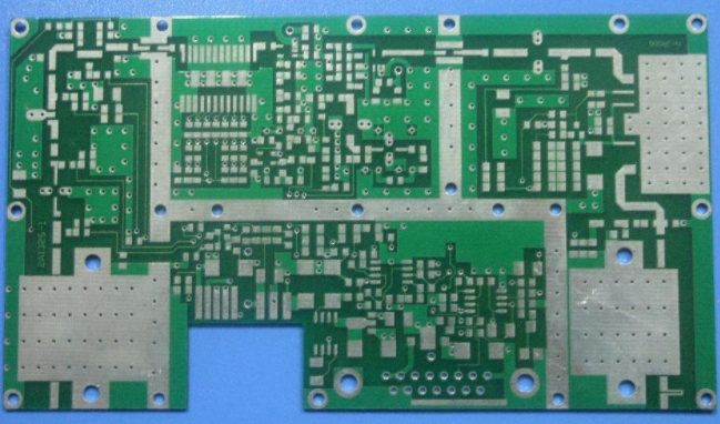
Printed Circuit Boards (PCBs) form the backbone of modern electronics, and as technology advances, the demand for high-difficulty PCBs continues to grow. These complex circuit boards push the boundaries of traditional PCB manufacturing, requiring specialized design approaches, advanced materials, and precision manufacturing techniques.
High-difficulty PCBs typically feature:
- Extremely high layer counts (often 20+ layers)
- Ultra-fine trace widths and spacing (below 3 mil)
- Microvias and advanced via technologies
- Mixed materials with different dielectric properties
- High-density interconnect (HDI) architectures
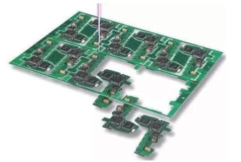
- Embedded components and passive elements
- Rigid-flex or flexible constructions
- Challenging thermal management requirements
These complex boards enable cutting-edge applications in aerospace, defense, medical devices, high-performance computing, and telecommunications equipment where conventional PCBs cannot meet the performance demands.
Design Challenges for Complex PCBs
Signal Integrity Considerations
High-difficulty PCBs often operate at GHz frequencies where signal integrity becomes paramount. Designers must carefully consider:
- Impedance control throughout the entire signal path
- Crosstalk mitigation between adjacent traces
- Proper termination techniques for high-speed signals
- Minimization of signal path discontinuities
- Careful management of return paths for high-frequency currents
Advanced simulation tools using 3D electromagnetic field solvers have become essential for predicting and optimizing signal behavior in these complex boards.
Power Delivery Network Design
Modern processors and ASICs require hundreds of amps at low voltages with tight regulation. This demands:
- Low-impedance power distribution networks
- Proper decoupling capacitor selection and placement
- Careful analysis of power plane resonances
- Effective management of simultaneous switching noise
- Consideration of DC voltage drop across the board
Thermal Management Strategies
High-power components in compact spaces create significant thermal challenges:
- Thermal via arrays under hot components
- Strategic placement of thermal reliefs
- Incorporation of metal cores or heatsinks
- Consideration of coefficient of thermal expansion (CTE) mismatches
- Advanced materials with high thermal conductivity
Manufacturing-Driven Design Rules
Designers must work closely with manufacturers to ensure designs are producible:
- Understanding fabrication capabilities and limitations
- Implementing proper via aspect ratios
- Providing adequate clearances for drilling and plating
- Accounting for material shrinkage and manufacturing tolerances
- Including proper testability features
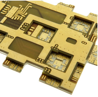
Advanced Materials for High-Performance PCBs
High-Frequency Laminates
For RF and microwave applications, materials with specific properties are required:
- Low dielectric constant (Dk) for faster signal propagation
- Low dissipation factor (Df) to minimize signal loss
- Stable electrical properties across frequency and temperature
- Common materials: Rogers RO4000 series, Taconic RF-35, Isola I-Tera
High-Temperature Materials
Applications in harsh environments demand:
- Polyimide-based substrates
- Ceramic-filled PTFE composites
- Materials with high glass transition temperatures (Tg)
- Low Z-axis expansion characteristics
Specialty Materials for Unique Applications
Emerging requirements drive material innovation:
- Low-loss materials for millimeter-wave applications
- Thermally conductive dielectrics for power electronics
- Flexible substrates for wearable electronics
- Transparent materials for display applications
Manufacturing Challenges and Solutions
Multilayer Lamination Processes
High-layer-count boards present unique manufacturing hurdles:
- Registration maintenance through multiple lamination cycles
- Prevention of resin starvation in thick stacks
- Management of interlayer stresses
- Void prevention in complex via structures
Microvia Formation
Advanced via technologies enable high-density interconnects:
- Laser-drilled microvias (typically < 100μm)
- Stacked and staggered via configurations
- Via-in-pad structures
- Filled and capped vias for planarization
Fine Line Fabrication
Achieving ultra-fine features requires:
- Advanced photolithography processes
- Modified semi-additive processes (mSAP)
- Direct imaging systems with high resolution
- Tight process control for etching uniformity
Controlled Impedance Manufacturing
Maintaining consistent impedance demands:
- Precise dielectric thickness control
- Tight tolerances on conductor width and spacing
- Careful material handling to prevent property changes
- Extensive testing and verification
Quality Assurance and Testing
Electrical Testing
Complex PCBs require rigorous testing:
- Flying probe or fixture-based continuity testing
- Time-domain reflectometry (TDR) for impedance verification
- High-voltage testing for insulation resistance
- RF testing for microwave boards
Non-Destructive Inspection
Advanced inspection techniques include:
- Automated optical inspection (AOI) at multiple stages
- X-ray inspection for buried and blind vias
- 3D computed tomography for complex structures
- Infrared inspection for thermal performance
Reliability Testing
Ensuring long-term reliability involves:
- Thermal cycling tests
- Vibration and mechanical shock testing
- Humidity and corrosion resistance testing
- Accelerated life testing
Applications of High-Difficulty PCBs
Aerospace and Defense
- Avionics systems
- Radar and electronic warfare equipment
- Satellite communications
- Guidance and control systems
Medical Electronics
- High-resolution imaging systems
- Implantable devices
- Surgical robotics
- Diagnostic equipment
High-Performance Computing
- Server motherboards
- Network switches and routers
- AI accelerator boards
- Supercomputing components
Telecommunications
- 5G infrastructure equipment
- Millimeter-wave systems
- Optical networking hardware
- Base station electronics
Future Trends in Complex PCB Technology
Embedded Components
Integration of passive and active components within the PCB structure:
- Embedded die technology
- Printed passive components
- Integrated voltage regulators
Advanced Packaging Technologies
Convergence of PCB and packaging approaches:
- Fan-out wafer-level packaging (FOWLP)
- Panel-level packaging
- Chiplets on substrate
Additive Manufacturing
Emerging 3D printing technologies for electronics:
- Fully additive PCB fabrication
- Printed electronics with novel materials
- Structural electronics integration
Sustainable Materials
Eco-friendly alternatives for high-performance PCBs:
- Bio-based resins
- Halogen-free materials
- Recyclable substrate systems
Conclusion
High-difficulty PCBs represent the cutting edge of electronic interconnection technology, enabling innovations across multiple industries. As electronic systems continue to demand higher performance in smaller form factors, the challenges in designing and manufacturing these complex boards will only increase. Success requires close collaboration between designers, material scientists, and manufacturing experts, along with continuous investment in new technologies and processes. The future of high-difficulty PCBs promises even greater integration, performance, and functionality, driving forward the capabilities of electronic systems in an increasingly connected world.