Requirements of PCBA Processing on Circuit Boards
Introduction
Printed Circuit Board Assembly (PCBA) is a critical process in electronics manufacturing, involving the placement and soldering of electronic components onto a printed circuit board (PCB). The quality and reliability of the final product depend heavily on how well the PCBA process adheres to specific requirements. This article explores the key requirements that PCBA processing imposes on circuit boards, covering design, material selection, manufacturing tolerances, surface finishes, and testing protocols.
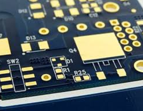
1. Design and Layout Requirements
The PCB design must align with PCBA processing capabilities to ensure smooth assembly. Key design considerations include:
1.1 Component Placement and Spacing
- Minimum Clearance: Sufficient space must be left between components to avoid soldering defects like bridging.
- Orientation: Components should be placed uniformly to facilitate automated pick-and-place machines.
- Thermal Considerations: High-power components need proper spacing to prevent overheating during soldering.
1.2 Pad and Trace Design
- Pad Size: Must match component leads to ensure proper solder joint formation.
- Trace Width: Adequate for current-carrying capacity while avoiding impedance issues.
- Via Placement: Vias should not obstruct solder paste application or reflow processes.
1.3 Panelization and Fiducial Marks
- Panel Design: PCBs are often panelized for batch processing; breakaway tabs must allow easy depanelization.
- Fiducial Marks: Required for automated assembly machines to ensure accurate component placement.
2. Material and Substrate Requirements
The choice of PCB material affects assembly performance and reliability.
2.1 Base Material Selection
- FR-4: Most common, suitable for standard applications.
- High-Frequency Materials: (e.g., Rogers, PTFE) for RF/microwave circuits.
- High-Tg Materials: For lead-free soldering and high-temperature applications.
2.2 Copper Thickness and Quality
- Copper Weight: Affects current handling and thermal dissipation.
- Surface Roughness: Smooth copper improves solderability.
2.3 Solder Mask and Silkscreen
- Solder Mask: Prevents solder bridging; must have proper alignment and thickness.
- Silkscreen: Must be legible for component identification without interfering with soldering.

3. Surface Finish Requirements
The PCB surface finish impacts solderability and shelf life.
3.1 Common Surface Finishes
- HASL (Hot Air Solder Leveling): Cost-effective but may cause uneven surfaces for fine-pitch components.
- ENIG (Electroless Nickel Immersion Gold): Flat surface, excellent for fine-pitch and BGA components.
- OSP (Organic Solderability Preservative): Eco-friendly but has limited shelf life.
- Immersion Silver/Tin: Good for high-frequency applications but prone to oxidation.
3.2 Finish Thickness and Durability
- Gold Thickness (ENIG): Typically 0.05–0.1µm to prevent brittle solder joints.
- OSP Coating: Must be uniform to prevent oxidation before assembly.
4. Manufacturing Tolerances and Process Control
PCBA demands tight tolerances to ensure consistency.
4.1 Dimensional Accuracy
- Drilling and Routing: Holes must align with component leads (±0.05mm tolerance).
- Layer Alignment: Misalignment can cause open/short circuits.
4.2 Solder Paste Application
- Stencil Thickness: Affects solder paste volume (typically 0.1–0.15mm).
- Aperture Design: Must match pad size to prevent insufficient or excessive solder.
4.3 Reflow and Wave Soldering Profiles
- Temperature Ramp Rates: Too fast/slow can cause defects like tombstoning or cold joints.
- Peak Temperature: Must suit both PCB material and component specifications.
5. Component Compatibility and Handling
PCBA requires proper component management.
5.1 Moisture Sensitivity Levels (MSL)
- Baking Requirements: Some ICs (e.g., BGAs) require pre-baking to avoid popcorning.
5.2 ESD Protection
- ESD-Safe Handling: Prevents static damage to sensitive components.
5.3 Component Packaging
- Tape-and-Reel vs. Trays: Must match pick-and-place machine feeders.
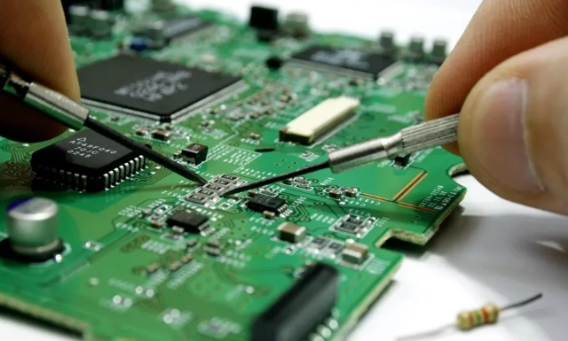
6. Testing and Quality Assurance
Post-assembly testing ensures reliability.
6.1 Automated Optical Inspection (AOI)
- Checks for solder defects, missing/misaligned components.
6.2 In-Circuit Testing (ICT) and Functional Testing
- Validates electrical performance and functionality.
6.3 X-Ray Inspection for BGAs and Hidden Joints
- Detects voids or cracks in solder balls.
7. Environmental and Regulatory Compliance
PCBA must meet industry standards.
7.1 RoHS and Lead-Free Requirements
- Lead-Free Solders: Require higher temperatures and process adjustments.
7.2 IPC Standards (IPC-A-610, IPC-J-STD-001)
- Define acceptable soldering and assembly quality.
7.3 Cleanliness and Contamination Control
- No-Clean Flux vs. Cleaning Requirements: Residue must be managed per application needs.
Conclusion
PCBA processing imposes stringent requirements on circuit boards, spanning design, materials, surface finishes, manufacturing tolerances, and testing protocols. By adhering to these requirements, manufacturers can ensure high yield, reliability, and compliance with industry standards. Continuous improvements in PCB technology and assembly techniques further enhance the efficiency and quality of PCBA production