Common Quality Issues in PCB Solder Mask Process and Their Solutions
Introduction
The solder mask process is a critical step in printed circuit board (PCB) manufacturing that serves multiple essential functions. Primarily applied to protect copper traces from oxidation and prevent solder bridges during component assembly, the solder mask also provides electrical insulation and enhances the board’s aesthetic appearance. Despite its importance, the solder mask application process is susceptible to various quality issues that can significantly impact PCB functionality and reliability.
This article examines the most common quality problems encountered during PCB solder mask application, analyzes their root causes, and provides practical solutions for prevention and correction. By understanding these issues and their remedies, manufacturers can improve product quality, reduce scrap rates, and enhance overall process efficiency.
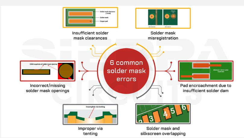
1. Solder Mask Misregistration
Problem Description
Solder mask misregistration occurs when the mask pattern does not align properly with the underlying copper features. This misalignment can result in exposed copper where coverage is needed or mask material covering pads that should remain exposed for soldering.
Causes
- Inaccurate artwork files: Discrepancies between design files and actual board dimensions
- Improper panel alignment: Errors during the panel alignment process before exposure
- Machine calibration issues: Malfunctioning or misaligned exposure equipment
- Material shrinkage: Dimensional changes in the substrate during curing
Solutions
- Verify artwork files against board specifications before production
- Implement regular calibration of exposure machines and alignment systems
- Use compensation factors to account for material shrinkage (typically 0.1-0.3%)
- Employ vision systems for precise alignment verification
- Consider using LDI (Laser Direct Imaging) technology for improved registration accuracy
2. Solder Mask Voids and Pinholes
Problem Description
Voids and pinholes are small, unintended openings in the solder mask layer that expose underlying copper surfaces. These defects can lead to corrosion, electrical leakage, or solder bridging during assembly.
Causes
- Contaminated copper surface: Presence of oxides, fingerprints, or processing residues
- Improper cleaning: Inadequate surface preparation before mask application
- Air entrapment: Bubbles formed during coating or developing processes
- Insufficient coating thickness: Mask layer too thin to provide complete coverage
Solutions
- Implement rigorous cleaning procedures (chemical cleaning, mechanical abrasion)
- Ensure proper drying after cleaning steps
- Optimize coating parameters (viscosity, speed, pressure) for complete coverage
- Use vacuum degassing for solder mask materials prone to bubble formation
- Implement multiple coating passes for critical applications
- Establish appropriate thickness measurement and control procedures
3. Solder Mask Peeling and Delamination
Problem Description
Peeling occurs when the solder mask separates from the PCB surface, potentially exposing copper traces or creating areas prone to contamination and corrosion.
Causes
- Poor adhesion: Inadequate bond between mask and copper/substrate
- Surface contamination: Residuals from previous processing steps
- Improper curing: Insufficient or excessive UV exposure and thermal curing
- Mechanical stress: Physical damage during handling or processing
- Material incompatibility: Mismatch between mask chemistry and board materials
Solutions
- Optimize surface preparation (micro-etching, plasma treatment)
- Verify compatibility between mask material and PCB substrate
- Establish proper curing parameters (intensity, duration, temperature)
- Implement adhesion promotion techniques (primers, surface activators)
- Conduct regular peel strength testing (ASTM D3359 standard)
- Avoid excessive mechanical stress during handling and processing
4. Solder Mask Bleeding
Problem Description
Bleeding refers to the unwanted flow of solder mask material onto areas meant to remain exposed, particularly solder pads. This defect can interfere with component soldering and lead to poor electrical connections.
Causes
- Excessive mask viscosity: Too low viscosity allowing material to flow
- Improper developing: Incomplete removal of unexposed mask material
- Overexposure: Excessive UV curing causing material hardening issues
- Design issues: Inadequate spacing between mask openings
Solutions
- Optimize mask viscosity for specific application methods
- Fine-tune developing parameters (time, temperature, pressure)
- Adjust exposure energy to manufacturer’s specifications
- Review design for adequate clearances (typically 0.05-0.1mm beyond pads)
- Implement edge-bumping techniques for tight tolerance areas
- Use higher resolution imaging techniques for fine feature definition
5. Incomplete Curing
Problem Description
Incomplete curing results in soft, tacky, or under-hardened solder mask that lacks proper chemical resistance and mechanical properties.
Causes
- Insufficient UV exposure: Low energy or short duration
- Improper thermal profile: Inadequate time/temperature in curing oven
- Shadowing effects: Masked areas receiving insufficient energy
- Old or degraded materials: Expired or improperly stored solder mask
Solutions
- Verify UV lamp intensity and output spectrum regularly
- Establish and monitor proper thermal curing profiles
- Implement dual-cure (UV+thermal) systems for complete polymerization
- Rotate boards during curing to eliminate shadowed areas
- Maintain strict material handling and storage procedures
- Conduct regular cure testing (acetone rub test, hardness measurement)
6. Solder Mask Discoloration
Problem Description
Discoloration manifests as uneven or unexpected color changes in the solder mask, which may indicate material degradation or processing issues.
Causes
- Overcuring: Excessive thermal or UV exposure
- Contamination: Chemical interactions with processing materials
- Material degradation: Age or improper storage conditions
- Incompatible chemicals: Exposure to harsh solvents or cleaners
Solutions
- Optimize curing parameters to avoid excessive exposure
- Implement proper material handling and storage procedures
- Verify compatibility of all processing chemicals
- Use UV-stable formulations for applications requiring color retention
- Establish controlled environments for sensitive materials
7. Orange Peel Texture
Problem Description
Orange peel refers to an uneven, textured surface resembling citrus peel, which can affect aesthetics and potentially interfere with fine-pitch component placement.
Causes
- Improper coating technique: Uneven application or drying
- Material viscosity issues: Incorrect formulation for application method
- Environmental factors: Temperature or humidity fluctuations
- Substrate effects: Underlying surface irregularities
Solutions
- Optimize coating parameters for smooth application
- Control environmental conditions (temperature 22±2°C, RH 50±5%)
- Use appropriate viscosity for selected coating method
- Consider substrate preparation to ensure smooth base surface
- Implement multiple thin coats rather than single heavy application
8. Solder Mask Thickness Variation
Problem Description
Inconsistent solder mask thickness across the PCB can lead to uneven protection, registration problems, and assembly issues.
Causes
- Uneven coating application: Inconsistent curtain, spray, or screen deposition
- Substrate warpage: Board deformation causing thickness variation
- Material flow: Improper leveling or settling after application
- Process parameter drift: Uncontrolled changes in application conditions
Solutions
- Regular maintenance and calibration of coating equipment
- Implement warpage control measures for substrates
- Use viscosity controls to maintain consistent material properties
- Establish thickness measurement points and monitoring procedures
- Consider alternative application methods for critical designs
Conclusion
The solder mask process presents numerous potential quality challenges, each capable of affecting PCB performance and reliability. By understanding the root causes of these common issues—including misregistration, voids, peeling, bleeding, incomplete curing, discoloration, orange peel texture, and thickness variation—manufacturers can implement targeted solutions to prevent and correct them.
Effective quality control in solder mask application requires a comprehensive approach combining material science, process engineering, and rigorous quality assurance practices. Key strategies include proper material selection, process parameter optimization, equipment maintenance, environmental control, and continuous operator training.
Implementing these solutions not only reduces defect rates but also enhances overall product quality and manufacturing efficiency. As PCB technology advances with finer features and more demanding applications, maintaining excellence in solder mask processing becomes increasingly critical for successful electronics manufacturing.