5G Technology: Considerations and Challenges for High-Speed PCB Design
Introduction
The advent of 5G technology has revolutionized wireless communication, offering unprecedented data speeds, ultra-low latency, and massive connectivity. However, the implementation of 5G networks and devices imposes stringent demands on high-speed printed circuit board (PCB) design. As signal frequencies escalate into the millimeter-wave (mmWave) spectrum (24 GHz and above), traditional PCB design methodologies face significant challenges in maintaining signal integrity, power efficiency, and thermal management.
This article explores the key considerations and challenges in designing high-speed PCBs for 5G applications, including material selection, signal integrity, power delivery, thermal management, and electromagnetic interference (EMI) mitigation.
1. Material Selection for High-Frequency PCBs
1.1 Dielectric Properties
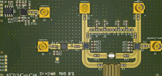
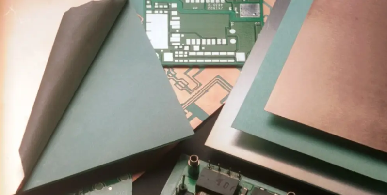
At high frequencies, the dielectric constant (Dk) and dissipation factor (Df) of PCB substrates become critical. Traditional FR-4 materials, while cost-effective, exhibit high signal loss at mmWave frequencies. Instead, high-frequency laminates such as Rogers RO4000, PTFE (Teflon), and hydrocarbon ceramics are preferred due to their low Dk and Df values.
- Low Dk ensures consistent signal propagation speed.
- Low Df minimizes dielectric losses, preserving signal strength.
1.2 Copper Roughness
As frequencies increase, skin effect—where current flows predominantly on the conductor’s surface—becomes more pronounced. Rough copper surfaces introduce additional insertion loss. Hence, high-speed PCBs use ultra-low-profile (ULP) copper foils to reduce conductor losses.
2. Signal Integrity Challenges
2.1 Impedance Control
5G signals operate at multi-gigabit rates, necessitating precise impedance matching (typically 50Ω for RF traces). Variations in trace width, dielectric thickness, or copper roughness can lead to impedance mismatches, causing reflections and signal degradation.
- Microstrip and Stripline Configurations: Careful modeling is required to maintain impedance.
- Differential Pair Routing: Ensures noise immunity in high-speed digital interfaces (e.g., PCIe, USB4).
2.2 Crosstalk and EMI Mitigation
Higher frequencies increase electromagnetic coupling between adjacent traces, leading to crosstalk. Techniques to mitigate crosstalk include:
- Increased trace spacing (3x the dielectric height).
- Ground shielding (via fences, coplanar waveguides).
- Differential signaling to cancel out common-mode noise.
2.3 Via Design and Signal Transition
Vias introduce discontinuities, causing signal reflections and losses. For mmWave PCBs:
- Use of back-drilled or blind/buried vias minimizes stub effects.
- Via-in-pad and microvias improve high-density interconnects (HDI).
3. Power Integrity and Distribution
3.1 Low-Impedance Power Delivery Network (PDN)
5G devices demand stable power delivery with minimal noise. Switching noise from high-speed processors and RF amplifiers can disrupt signal integrity. Key strategies include:
- Multi-layer PCBs with dedicated power and ground planes.
- Decoupling capacitors placed near ICs to suppress high-frequency noise.
- Low-inductance power planes to minimize voltage fluctuations.
3.2 High-Current Power Rails
Advanced 5G chips (e.g., RF power amplifiers, FPGAs) require high current, leading to IR drops and thermal issues. Solutions include:
- Wider power traces and thicker copper layers (2 oz or more).
- Thermal vias to dissipate heat efficiently.
4. Thermal Management Considerations
4.1 Heat Dissipation in High-Power 5G PCBs
5G base stations and mmWave devices generate substantial heat due to high-frequency operation. Poor thermal management can degrade performance and reliability.
- Thermal vias and heatsinks improve heat dissipation.
- Metal-core PCBs (MCPCBs) or insulated metal substrates (IMS) for high-power RF sections.
- Thermal simulation tools (e.g., ANSYS, Flotherm) optimize heat distribution.
4.2 Coefficient of Thermal Expansion (CTE) Mismatch
Different materials expand at varying rates under heat, leading to mechanical stress. Using materials with matched CTE (e.g., copper and ceramic-filled PTFE) prevents delamination.
5. Manufacturing and Assembly Challenges
5.1 Tight Tolerances in High-Frequency PCBs
mmWave PCBs require ultra-precise fabrication:
- Laser drilling for microvias (<100µm).
- Controlled impedance tolerances within ±5%.
- High-precision etching to maintain trace uniformity.
5.2 Assembly and Rework Difficulties
- Fine-pitch BGAs and QFNs complicate soldering.
- Low-temperature solders prevent laminate damage.
- Automated optical inspection (AOI) ensures defect-free assembly.
6. Future Trends in 5G PCB Design
6.1 Integration of AI and Machine Learning
AI-driven design tools optimize signal routing, PDN analysis, and thermal management.
6.2 Advanced Packaging Technologies
- System-in-Package (SiP) and fan-out wafer-level packaging (FOWLP) reduce interconnect lengths.
- Embedded active/passive components minimize parasitic effects.
6.3 6G and Beyond: Terahertz PCBs
As research progresses toward 6G (sub-THz frequencies), new materials (e.g., liquid crystal polymers) and waveguide-integrated PCBs will emerge.

Conclusion
Designing high-speed PCBs for 5G technology presents multifaceted challenges, from material selection to thermal and signal integrity management. Engineers must leverage advanced simulation tools, high-frequency laminates, and innovative manufacturing techniques to meet the demands of next-generation wireless systems. As 5G evolves into 6G, PCB design will continue to push the boundaries of high-frequency electronics, enabling faster, more reliable connectivity.
By addressing these considerations proactively, PCB designers can ensure robust performance in 5G applications, paving the way for future advancements in wireless communication.