Common Problems in PCB Application and Their Solutions
Introduction
Printed Circuit Boards (PCBs) form the backbone of modern electronics, serving as the platform that connects and supports various electronic components. As technology advances and electronic devices become more complex, PCBs have evolved from simple single-layer boards to sophisticated multi-layer designs with high-density interconnects. However, this complexity brings numerous challenges in PCB application. This article explores the most common problems encountered during PCB design, manufacturing, assembly, and operation, providing insights into their causes and potential solutions.
Understanding these common PCB issues is crucial for electronics engineers, designers, and manufacturers. By recognizing these problems early and implementing appropriate solutions, professionals can significantly improve product reliability, reduce production costs, and shorten time-to-market. The discussion will cover design-related issues, manufacturing defects, assembly challenges, and operational failures, offering a comprehensive view of PCB application problems across the entire product lifecycle.
Design-Related Problems
1. Incorrect Footprint and Package Selection
One of the most frequent design mistakes involves selecting wrong component footprints or packages. This occurs when the physical dimensions or pin configuration in the PCB layout don’t match the actual components intended for assembly. The consequences can range from minor rework requirements to complete board failures.
Solutions:
- Always verify component datasheets before creating footprints
- Use verified library parts from reputable sources
- Implement a peer-review process for critical components
- Create physical prototypes to validate footprints before full production
2. Insufficient Clearance and Creepage Distances
Electrical clearance (shortest distance through air) and creepage (shortest distance along surface) are critical for preventing arcing and ensuring product safety, especially in high-voltage applications. Many designers underestimate these requirements, leading to potential safety hazards or non-compliance with regulations.
Solutions:
- Consult relevant safety standards (IEC, UL, etc.) for specific requirements
- Use design rule checking (DRC) tools with appropriate clearance settings
- Consider environmental factors like humidity and pollution degree
- Implement proper slotting or barriers in high-voltage areas
3. Poor Thermal Management
Inadequate thermal design leads to overheating components, reduced reliability, and premature failures. Common issues include insufficient copper for heat dissipation, poor component placement, and lack of thermal vias under high-power devices.
Solutions:
- Conduct thermal analysis during design phase
- Use thermal relief patterns appropriately
- Implement proper copper pour and thermal vias
- Consider heat sinks or active cooling for high-power components
- Follow manufacturer’s recommendations for thermal pad designs
4. Signal Integrity Issues
With increasing clock speeds and edge rates, signal integrity problems like reflections, crosstalk, and electromagnetic interference (EMI) have become more prevalent. These issues often manifest as intermittent operation or complete system failures.
Solutions:
- Maintain proper impedance control for critical traces
- Implement appropriate termination strategies
- Minimize parallel run lengths between sensitive signals
- Use ground planes effectively for return paths
- Consider differential signaling for high-speed interfaces
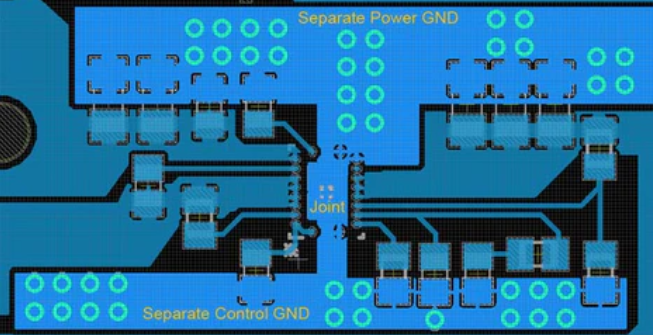
5. Inadequate Power Distribution
Poor power distribution network (PDN) design can lead to voltage drops, ground bounce, and excessive noise, particularly in digital systems with high current transients.
Solutions:
- Use appropriate decoupling capacitor strategy
- Implement proper power and ground plane structures
- Consider the use of power integrity analysis tools
- Ensure adequate copper weight for high-current paths
- Implement proper star-point grounding when necessary
Manufacturing Defects
1. Copper Etching Problems
Etching issues during PCB fabrication can result in under-etched (shorts) or over-etched (open circuits) traces, affecting board functionality.
Solutions:
- Work with reputable PCB manufacturers
- Ensure proper etch compensation in design
- Specify appropriate copper weights for current requirements
- Implement proper design rules for minimum trace/space
2. Drilling and Plating Defects
Problems with via drilling and plating can lead to unreliable connections between layers, particularly in high-density designs with small vias.
Solutions:
- Follow manufacturer’s capabilities for minimum via sizes
- Specify appropriate plating thickness requirements
- Consider via fill options for critical applications
- Implement proper via design rules (aspect ratios, etc.)
3. Solder Mask Issues
Improper solder mask application can cause bridging between pads or insufficient protection, leading to potential shorts or corrosion.
Solutions:
- Specify appropriate solder mask expansion values
- Ensure proper solder mask dam between fine-pitch components
- Consider solder mask color selection based on inspection needs
- Verify solder mask registration tolerances with manufacturer
4. Warpage and Dimensional Instability
PCB warpage can cause assembly problems and reliability issues, particularly in large boards or those exposed to thermal cycling.
Solutions:
- Maintain symmetrical layer stackup to prevent inherent warpage
- Specify appropriate board materials for the application
- Consider panelization strategies to improve handling
- Follow proper storage and handling procedures
5. Surface Finish Problems
The choice and quality of surface finish (ENIG, HASL, OSP, etc.) can significantly affect solderability and long-term reliability.
Solutions:
- Select surface finish appropriate for the application and components
- Specify thickness requirements for finishes like ENIG
- Consider shelf-life requirements when choosing finishes
- Implement proper storage conditions for PCBs before assembly
Assembly Challenges
1. Solder Bridging
Solder bridges between adjacent pins, particularly in fine-pitch components, remain a common assembly defect.
Solutions:
- Optimize solder paste stencil design (aperture size, shape)
- Implement proper solder mask between pads
- Adjust reflow profile parameters
- Consider nitrogen atmosphere for difficult assemblies
2. Tombstoning (Component Lifting)
Small passive components (like 0402 or smaller) may lift on one end during reflow, creating open circuits.
Solutions:
- Ensure symmetrical pad and thermal relief design
- Balance copper area on both ends of components
- Optimize reflow temperature profile
- Consider solder paste volume adjustments
3. Voiding in Solder Joints
Voids in solder joints, particularly in BGA packages or large thermal pads, can compromise thermal and electrical performance.
Solutions:
- Implement proper thermal via design under pads
- Optimize stencil design for paste deposition
- Consider vacuum reflow for critical applications
- Use X-ray inspection to verify void percentages
4. Component Misalignment
Misaligned components can cause shorts or open connections, particularly with fine-pitch devices.
Solutions:
- Ensure proper fiducial marker design
- Verify pick-and-place machine calibration
- Consider component packaging (tape-and-reel vs. tray)
- Implement optical inspection systems
5. Moisture Sensitivity Issues
Moisture-sensitive components can suffer from “popcorning” or internal delamination during reflow if not properly handled.
Solutions:
- Implement proper moisture control procedures
- Follow manufacturer’s baking requirements when needed
- Use moisture barrier bags with humidity indicators
- Consider component drying before assembly
Operational Failures
1. Electromigration
Over time, high current density can cause metal atoms to migrate, eventually leading to open circuits or increased resistance.
Solutions:
- Design traces with adequate current-carrying capacity
- Consider environmental factors (temperature, humidity)
- Implement redundancy for critical paths
- Use conformal coating in harsh environments
2. Conductive Anodic Filament (CAF) Formation
CAF involves the growth of conductive filaments along the glass fibers in the PCB laminate, causing insulation resistance degradation.
Solutions:
- Use CAF-resistant laminate materials
- Maintain proper spacing between biased conductors
- Control humidity exposure
- Consider conformal coating for humid environments
3. Thermal Cycling Failures
Repeated thermal expansion and contraction can cause solder joint cracks or plated through-hole barrel cracks.
Solutions:
- Match coefficients of thermal expansion (CTE) where possible
- Use appropriate via fill materials
- Implement strain relief for large components
- Consider underfill for BGA packages in harsh environments
4. Corrosion
Environmental exposure can lead to corrosion of metal surfaces, particularly in high-humidity or contaminated atmospheres.
Solutions:
- Select appropriate surface finishes
- Implement conformal coating
- Design for proper drainage in exposed environments
- Consider hermetic sealing for extreme conditions
5. Mechanical Stress Failures
Physical stress from vibration, shock, or flexing can damage components or PCB interconnects.
Solutions:
- Implement proper board support and mounting
- Use strain relief for connectors
- Consider flexible PCBs or rigid-flex designs where appropriate
- Avoid placing heavy components in high-stress areas
Testing and Quality Assurance Challenges
1. Inadequate Test Coverage
Many PCB failures result from insufficient testing strategies that fail to catch potential defects.
Solutions:
- Implement comprehensive design-for-test (DFT) practices
- Use a combination of in-circuit and functional testing
- Consider boundary scan for complex assemblies
- Develop proper test fixtures and procedures
2. False Test Results
Test equipment or methodology issues can lead to false passes or false failures, compromising quality.
Solutions:
- Regularly calibrate test equipment
- Validate test programs with known-good and known-bad boards
- Implement proper fixture maintenance procedures
- Consider environmental factors during testing
3. Difficulty in Fault Isolation
Complex multi-layer boards can make fault isolation extremely challenging when failures occur.
Solutions:
- Implement test points for critical signals
- Consider built-in self-test (BIST) features
- Use automated optical inspection (AOI) and X-ray systems
- Develop systematic troubleshooting procedures
Conclusion
PCB application involves numerous potential pitfalls spanning design, manufacturing, assembly, and operation. The problems discussed in this article represent common challenges faced by electronics professionals across industries. By understanding these issues and implementing the suggested solutions, engineers and manufacturers can significantly improve PCB reliability and yield.
Prevention remains the most effective strategy for addressing PCB problems. Investing in proper design practices, thorough design reviews, and collaboration with manufacturing partners early in the development process can prevent many issues before they occur. Additionally, implementing robust testing and quality assurance procedures helps catch remaining problems before products reach the field.
As PCB technology continues to evolve with trends like higher densities, flexible circuits, and embedded components, new challenges will undoubtedly emerge. Staying informed about these developments and maintaining a proactive approach to problem-solving will be essential for success in the ever-changing landscape of PCB applications.
Ultimately, the key to minimizing PCB problems lies in a holistic approach that considers the entire product lifecycle, from initial concept through end-of-life. By combining sound engineering principles with lessons learned from past failures, electronics professionals can continue to push the boundaries of what’s possible while maintaining the reliability that modern applications demand.