Understanding Voltage Drop in PCB Design: Causes, Effects, and Mitigation Strategies
Introduction
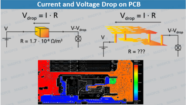
Voltage drop is a critical consideration in printed circuit board (PCB) design, particularly in high-current and high-speed applications. When current flows through a conductor (such as a PCB trace), resistance in the conductor causes a reduction in voltage along its length. Excessive voltage drop can lead to performance degradation, signal integrity issues, and even circuit failure. This article explores the causes of voltage drop in PCB design, its effects on circuit performance, and effective strategies to mitigate it.
1. Causes of Voltage Drop in PCB Design
Voltage drop occurs due to several factors related to PCB layout, material properties, and electrical characteristics. The primary causes include:
1.1 Trace Resistance
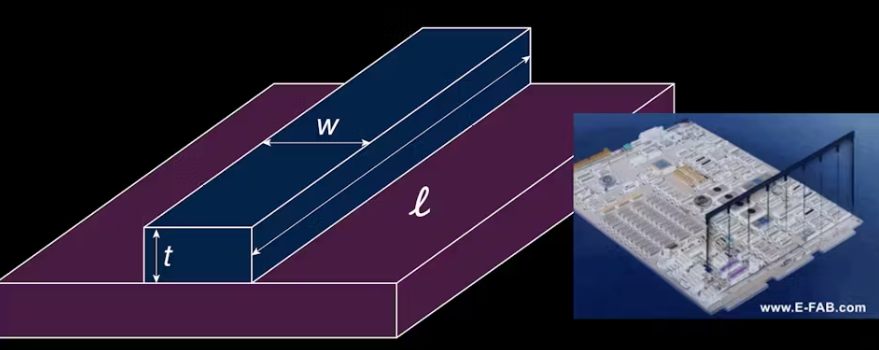
The inherent resistance of PCB traces contributes significantly to voltage drop. The resistance of a trace is determined by:
- Trace width and thickness: Narrow or thin traces have higher resistance.
- Trace length: Longer traces increase resistance.
- Copper weight (oz/ft²): Thinner copper layers (e.g., 0.5 oz) have higher resistance than thicker ones (e.g., 2 oz).
The resistance of a PCB trace can be calculated using:
[
R = \rho \cdot \frac{L}{A}
]
where:
- ( R ) = Resistance (Ω)
- ( \rho ) = Resistivity of copper (1.68 × 10⁻⁸ Ω·m)
- ( L ) = Trace length (m)
- ( A ) = Cross-sectional area (width × thickness, m²)
1.2 High Current Flow
Ohm’s Law (( V = I \cdot R )) shows that voltage drop increases with higher current. Power-hungry components (e.g., processors, FPGAs, motors) exacerbate voltage drop if traces are not adequately sized.
1.3 Via Resistance
Vias introduce additional resistance, especially in multi-layer PCBs. Poorly designed vias (small diameter, excessive length) increase voltage drop.
1.4 Poor Power Distribution Network (PDN) Design
- Insufficient power planes or thin power traces.
- Inadequate decoupling capacitors leading to transient voltage drops.
- Long return paths increasing ground resistance.
1.5 Temperature Effects
Copper resistance increases with temperature, worsening voltage drop in high-power applications.
2. Effects of Voltage Drop on PCB Performance
Excessive voltage drop can lead to several operational issues:
2.1 Reduced Signal Integrity
- Digital circuits: Voltage drops can cause logic errors if supply voltage falls below the minimum threshold.
- Analog circuits: Sensitive analog components (e.g., ADCs, amplifiers) may exhibit noise or distortion.
2.2 Power Supply Instability
- Voltage-sensitive components (e.g., microcontrollers) may reset or malfunction.
- Switching regulators may struggle to maintain stable output.
2.3 Increased Power Dissipation
- Higher resistance leads to ( I²R ) losses, generating heat and reducing efficiency.
2.4 EMI and Ground Bounce Issues
- Uneven power distribution can cause ground loops and electromagnetic interference (EMI).
3. Mitigation Strategies for Voltage Drop in PCB Design
To minimize voltage drop, designers should implement the following best practices:
3.1 Optimize Trace Width and Thickness
- Use PCB trace width calculators to determine appropriate dimensions based on current requirements.
- Wider traces reduce resistance (e.g., 50 mil traces for 5A current).
- Increase copper weight (e.g., 2 oz instead of 1 oz) for high-current paths.
3.2 Minimize Trace Length
- Place high-current components close to power sources.
- Use star topology for power distribution to avoid long daisy-chained traces.
3.3 Use Power and Ground Planes
- Dedicated power planes reduce resistance and inductance.
- Multiple vias connecting planes improve current distribution.
3.4 Reduce Via Resistance
- Use larger via diameters (e.g., 0.3 mm instead of 0.2 mm).
- Multiple vias in parallel for high-current paths.
3.5 Implement Proper Decoupling Capacitors
- Place decoupling capacitors near power pins to stabilize voltage.
- Use bulk capacitors for transient current demands.
3.6 Thermal Management
- Ensure proper heat dissipation to prevent resistance increase.
- Use thermal vias for heat transfer in high-power areas.
3.7 Simulation and Analysis
- Use SPICE simulations or PDN analyzers (e.g., Ansys SIwave, Cadence Sigrity) to predict voltage drop.
- Perform DC IR drop analysis to identify critical paths.
4. Practical Example: Calculating Voltage Drop
Consider a 5V power trace supplying 3A to an IC:
- Trace dimensions: 10 cm long, 20 mils wide, 1 oz copper.
- Resistance calculation:
[
R = \rho \cdot \frac{L}{A} = 1.68 \times 10^{-8} \cdot \frac{0.1}{(0.02 \times 0.000035)} \approx 0.024 \, \Omega
] - Voltage drop:
[
V_{drop} = I \cdot R = 3 \times 0.024 = 0.072 \, V
] - Resulting voltage at load:
[
V_{load} = 5V – 0.072V = 4.928V
]
If the IC requires a minimum of 4.8V, this design is acceptable. However, for tighter tolerances, wider traces or thicker copper may be needed.
5. Conclusion
Voltage drop in PCB design is an unavoidable phenomenon, but with careful planning, its impact can be minimized. By optimizing trace geometry, using power planes, reducing via resistance, and performing simulations, designers can ensure stable power delivery and reliable circuit operation. Understanding and mitigating voltage drop is essential for high-performance, high-reliability PCB designs in modern electronics.