Failure Mechanisms Behind Poor Solder Melting Phenomena in PCBs
Abstract
Poor solder melting (or “cold solder”) is a common defect in printed circuit board (PCB) assembly, leading to weak joints, intermittent connections, and eventual circuit failure. This paper explores the underlying failure mechanisms behind poor solder melting, including metallurgical factors, process-related issues, and environmental influences. By analyzing root causes such as oxidation, insufficient thermal energy, contamination, and intermetallic compound (IMC) formation, this study provides insights into mitigation strategies to improve soldering reliability in PCB manufacturing.
1. Introduction
Soldering is a critical process in PCB assembly, ensuring electrical and mechanical connections between components and the board. Poor solder melting—where solder fails to properly wet or adhere to pads or leads—results in defective joints that compromise performance. Understanding the failure mechanisms behind this phenomenon is essential for improving manufacturing yield and long-term reliability.
This paper examines key factors contributing to poor solder melting, including:
- Oxidation and contamination
- Insufficient thermal energy transfer
- Intermetallic compound (IMC) formation
- Flux activity and solder alloy composition
- Process-related defects (reflow profile, solder paste quality)
2. Metallurgical and Chemical Factors
2.1 Oxidation of Surfaces
Oxidation is a primary cause of poor solder wetting. Copper pads and component leads form oxide layers (Cu₂O, CuO) when exposed to air, preventing proper solder adhesion. Similarly, solder powder in paste can oxidize, reducing its melting efficiency.
Failure Mechanism:
- Oxide layers act as barriers, inhibiting metallurgical bonding.
- High-temperature oxidation accelerates during reflow if the atmosphere (e.g., nitrogen vs. air) isn’t controlled.
Mitigation:
- Use no-clean or activated fluxes to remove oxides.
- Store PCBs and components in moisture-controlled environments.
- Optimize reflow atmosphere (e.g., nitrogen inerting).
2.2 Contamination on PCB or Components
Contaminants such as oils, dust, or residues from fabrication (e.g., solder mask, plating chemicals) can hinder solder wetting.
Failure Mechanism:
- Organic residues decompose during reflow, creating non-wettable surfaces.
- Ionic contamination (e.g., chlorides, sulfates) promotes electrochemical migration.
Mitigation:
- Implement thorough PCB cleaning before assembly.
- Verify compatibility between solder mask and soldering processes.
3. Thermal Energy and Process-Related Issues
3.1 Insufficient Heat Transfer
Poor solder melting often occurs due to uneven or inadequate heating during reflow.
Failure Mechanism:
- Large thermal masses (e.g., ground planes) act as heat sinks, preventing solder from reaching melting temperature.
- Incorrect reflow profile (too short or low peak temperature) leads to incomplete melting.
Mitigation:
- Adjust reflow profile (preheat, soak, peak temperature) based on PCB design.
- Use thermal reliefs in pad designs to balance heat distribution.
3.2 Solder Paste Quality and Application
Poor solder paste properties (e.g., low metal content, expired paste) or improper stencil printing can cause melting defects.
Failure Mechanism:
- Solder paste slump or misalignment leads to uneven reflow.
- Aged solder paste (oxidized powder) reduces wetting ability.
Mitigation:
- Monitor solder paste viscosity and storage conditions.
- Optimize stencil thickness and aperture design.
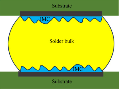
4. Intermetallic Compound (IMC) Formation
IMC layers (e.g., Cu₆Sn₅, Cu₃Sn) form at solder-copper interfaces, but excessive or brittle IMC growth weakens joints.
Failure Mechanism:
- Thick IMC layers (due to prolonged high temperatures) reduce mechanical strength.
- Kirkendall voids form due to uneven diffusion, increasing fracture risk.
Mitigation:
- Control reflow time and temperature to limit IMC growth.
- Use solder alloys with additives (e.g., Ni, Bi) to suppress brittle IMC formation.
5. Flux Activity and Solder Alloy Composition
5.1 Flux Inefficiency
Flux removes oxides and promotes wetting, but insufficient activity leads to poor melting.
Failure Mechanism:
- Low-activity flux fails to remove oxides, especially in lead-free (Sn-Ag-Cu) solders.
- Flux burnout occurs if preheat is too long.
Mitigation:
- Select flux with appropriate activity for the application (e.g., RA vs. RMA).
- Optimize reflow profile to match flux activation.
5.2 Solder Alloy Selection
Lead-free alloys (e.g., SAC305) have higher melting points than traditional Sn-Pb, requiring tighter process control.
Failure Mechanism:
- High surface tension of lead-free solder reduces wetting.
- Alloy segregation (e.g., Sn-rich zones) creates inconsistent melting.
Mitigation:
- Use alloys with wetting enhancers (e.g., Ge, Ni).
- Adjust reflow parameters for lead-free compatibility.
6. Environmental and Storage Factors
6.1 Moisture Sensitivity
Moisture absorption in PCBs or components (e.g., “popcorning” in ICs) can disrupt soldering.
Failure Mechanism:
- Steam generation during reflow causes voids or splattering.
- Moisture accelerates oxidation of pads and solder.
Mitigation:
- Bake moisture-sensitive components before assembly.
- Store PCBs in dry environments.
7. Conclusion
Poor solder melting in PCBs arises from multiple interrelated factors, including oxidation, contamination, thermal management, flux activity, and alloy properties. Addressing these issues requires a holistic approach:
- Process Optimization: Reflow profile tuning, proper solder paste handling.
- Material Selection: High-quality fluxes, compatible alloys.
- Design Considerations: Thermal reliefs, pad finishes (e.g., ENIG, OSP).
By understanding these failure mechanisms, manufacturers can improve solder joint reliability and reduce defects in PCB assembly.