PCB Antenna Design: Principles, Techniques, and Practical Considerations
Introduction to PCB Antennas
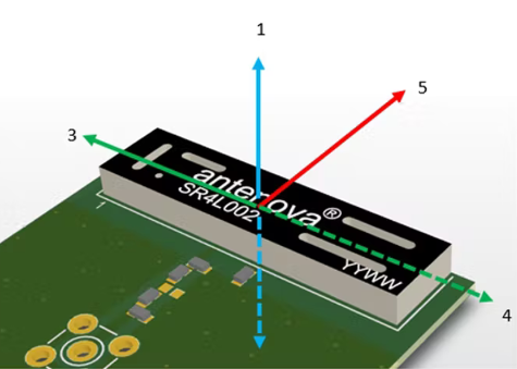
Printed Circuit Board (PCB) antennas have become increasingly popular in modern wireless communication systems due to their compact size, low cost, and ease of integration with electronic circuits. These antennas are fabricated directly onto the PCB substrate, eliminating the need for separate antenna components and reducing assembly complexity. PCB antennas are widely used in applications such as WiFi, Bluetooth, Zigbee, RFID, cellular IoT devices, and various other wireless technologies operating from MHz to GHz frequency ranges.
The fundamental advantage of PCB antennas lies in their seamless integration with the rest of the electronic system. Unlike external antennas that require connectors and additional assembly steps, PCB antennas are etched directly onto the board during the standard PCB manufacturing process. This integration results in reduced component count, lower production costs, and improved reliability by eliminating mechanical connection points that could fail over time.
Basic Principles of PCB Antenna Design
Electromagnetic Fundamentals
PCB antennas operate on the same basic principles as conventional antennas, converting electrical signals into electromagnetic waves (transmission) and vice versa (reception). The key parameters that characterize antenna performance include:
- Resonance Frequency: The frequency at which the antenna exhibits maximum efficiency, determined by its physical dimensions and the dielectric properties of the PCB material.
- Impedance Matching: The antenna’s input impedance (typically 50Ω for RF systems) must match the transmission line impedance to minimize signal reflections.
- Bandwidth: The range of frequencies over which the antenna maintains acceptable performance, usually defined by parameters such as VSWR < 2:1 or return loss > 10 dB.
- Radiation Pattern: The directional characteristics of the radiated electromagnetic field, describing how energy is distributed in three-dimensional space.
- Gain: A measure of the antenna’s ability to concentrate radiated power in particular directions compared to an isotropic radiator.
- Efficiency: The ratio of radiated power to input power, accounting for losses in conductors and dielectric materials.
PCB Material Considerations
The choice of PCB material significantly impacts antenna performance. Key parameters include:
- Dielectric Constant (εr): Affects the electrical length of the antenna and its resonant frequency. Common FR4 material has εr ≈ 4.3-4.8, while high-frequency laminates like Rogers materials offer lower and more stable εr values.
- Loss Tangent (tanδ): Determines dielectric losses, with lower values preferred for better efficiency. FR4 has relatively high loss (tanδ ≈ 0.02) compared to specialized RF materials (tanδ ≈ 0.001-0.005).
- Substrate Thickness: Influences bandwidth and impedance characteristics. Thicker substrates generally provide wider bandwidth but may increase unwanted surface wave effects.
- Copper Thickness: Affects conductor losses and current-carrying capacity. Standard 1 oz/ft² (35 μm) copper is common, but thicker copper can reduce resistive losses.
Common PCB Antenna Types
1. Microstrip Patch Antennas
Microstrip patch antennas consist of a radiating patch on one side of the dielectric substrate with a ground plane on the opposite side. These antennas offer several advantages:
- Design simplicity: Rectangular, circular, or other geometric shapes can be easily fabricated
- Low profile: Typically λ₀/2 or less in thickness
- Conformal mounting: Can be adapted to curved surfaces
- Array capability: Multiple patches can be arranged to form phased arrays
The resonant frequency of a rectangular patch antenna is approximately given by:
fᵣ = c / [2(L + ΔL)√(εₑff)]
where c is the speed of light, L is the patch length, ΔL accounts for fringing effects, and εₑff is the effective dielectric constant.
2. Inverted-F Antennas (IFA)
IFA antennas are popular for compact wireless devices due to their small size and reasonable performance:
- Space-efficient: Typically λ/4 in length
- Ground plane dependent: Performance relies on proper ground plane dimensions
- Omnidirectional pattern: Suitable for applications requiring non-directional coverage
The IFA consists of a radiating element parallel to the ground plane, a shorting stub to ground, and a feed point that determines the input impedance.
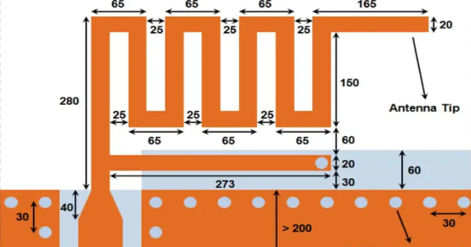
3. Meandered Line Antennas
Meandered line antennas use a serpentine pattern to reduce the overall antenna size while maintaining the required electrical length:
- Size reduction: Can achieve up to 50-70% size reduction compared to straight counterparts
- Trade-offs: Reduced bandwidth and efficiency compared to full-size antennas
- Design complexity: Requires careful optimization of meander parameters (width, spacing, turns)
4. Planar Inverted-F Antennas (PIFA)
PIFA antennas combine features of patch and IFA designs:
- Low profile: Height typically λ/8 to λ/12
- Bandwidth control: Can be adjusted through design parameters
- Ground plane integration: Requires careful consideration of ground plane size
5. Dipole and Monopole PCB Antennas
PCB implementations of these classic antenna types:
- Dipole: Requires balanced feed, typically λ/2 total length
- Monopole: Requires ground plane, λ/4 length
- Printed versions: Can be implemented as traces on the PCB with appropriate feeding
Design Considerations and Optimization Techniques
Impedance Matching
Proper impedance matching is crucial for maximizing power transfer between the RF circuitry and antenna. Common techniques include:
- Matching Networks: LC networks (L-section, π-network, T-network) can transform impedance to the desired value
- Stub Matching: Open or shorted transmission line stubs provide reactive compensation
- Tapered Transitions: Gradual width changes can match impedances over broad bandwidths
Ground Plane Effects
The ground plane significantly influences PCB antenna performance:
- Size: Should be at least λ/4 at the operating frequency for proper monopole operation
- Shape: Irregular shapes can distort radiation patterns
- Clearance: Keep antenna area free of other components and ground pour
- Current Return Path: Ensure low-impedance return paths for RF currents
Miniaturization Techniques
When space is constrained, several techniques can reduce antenna size:
- High-εr Materials: Increase electrical length for given physical dimensions
- Loading Techniques: Use lumped elements (capacitors, inductors) to reduce size
- Fractal Geometries: Exploit self-similar patterns to maximize length in limited area
- Slot Antennas: Use slots in ground plane as radiating elements
Multi-band Design
For devices operating at multiple frequencies:
- Harmonic Designs: Create structures resonant at multiple harmonics
- Parasitic Elements: Add coupled elements tuned to different frequencies
- Reconfigurable Antennas: Use switches or tunable components to alter characteristics
Practical Implementation Guidelines
Layout Considerations
- Keep-out Areas: Maintain clearance around the antenna (typically λ/4 minimum)
- Component Placement: Avoid placing components, especially metals, near the antenna
- Feed Line Design: Use controlled impedance traces with proper width calculation
- Via Placement: Minimize vias near the antenna; use stitching vias for ground continuity
Simulation and Verification
Modern PCB antenna design relies heavily on electromagnetic simulation:
- 3D EM Solvers: Tools like HFSS, CST, or ADS Momentum provide accurate performance prediction
- Parametric Studies: Analyze sensitivity to key dimensions and material properties
- Co-simulation: Combine circuit and EM simulation for complete system analysis
- Prototyping: Verify performance with network analyzer measurements (S11, radiation patterns)
Manufacturing Considerations
- Tolerances: Account for fabrication variations (typically ±0.1mm for PCB features)
- Copper Roughness: Surface roughness affects high-frequency performance
- Solder Mask: Can slightly affect dielectric properties; may need modeling
- Assembly Effects: Components and enclosures can detune the antenna
Advanced Topics in PCB Antenna Design
MIMO and Antenna Arrays
Modern wireless systems often employ Multiple Input Multiple Output (MIMO) techniques:
- Isolation Techniques: Ensure low coupling between antenna elements (λ/2 spacing, polarization diversity, pattern diversity)
- Decoupling Networks: Implement circuits to reduce mutual coupling
- Beamforming: Phased arrays for directional gain and spatial multiplexing
Flexible and Stretchable PCB Antennas
Emerging applications in wearable electronics require:
- Flexible Substrates: Polyimide or other bendable materials
- Stretchable Designs: Meandered or helical structures that maintain performance when stretched
- Conformal Integration: Antennas that adapt to non-planar surfaces
Metamaterial-inspired Antennas
Novel designs incorporating metamaterial concepts:
- Electrically Small Antennas: Using metamaterials to overcome fundamental size limitations
- Enhanced Bandwidth: Metamaterial loading for wider operating bandwidth
- Pattern Control: Tailoring radiation characteristics with metamaterial structures
Conclusion
PCB antenna design represents a crucial enabling technology for modern wireless systems, offering compact, cost-effective solutions with good performance characteristics. Successful design requires careful consideration of electromagnetic principles, material properties, layout constraints, and system integration factors. While basic antenna types like microstrip patches and IFAs provide good starting points, advanced techniques such as MIMO implementations, metamaterial loading, and flexible designs continue to push the boundaries of what’s possible with PCB-based antennas.
As wireless technology evolves toward higher frequencies (mmWave for 5G/6G) and more compact form factors, PCB antenna design will remain a vital area of innovation. Future developments may include more sophisticated integration with active components, improved materials with lower loss and more stable properties, and AI-driven optimization techniques for rapid design iteration. By mastering the fundamentals and staying abreast of emerging trends, engineers can create PCB antenna solutions that meet the demanding requirements of next-generation wireless devices.