Optimizing PCB Routing to Reduce Crosstalk
Abstract
This paper explores the critical aspects of crosstalk in printed circuit board (PCB) designs and provides comprehensive strategies for minimizing interference through optimized routing techniques. As electronic devices continue to increase in complexity and operating frequencies, managing crosstalk has become essential for ensuring signal integrity and reliable system performance. The article examines the fundamental causes of crosstalk, analyzes its effects on signal quality, and presents practical design approaches to mitigate this pervasive issue in modern PCB layouts.
Introduction
In today’s high-speed electronic systems, crosstalk represents one of the most significant challenges to signal integrity. With clock speeds exceeding gigahertz ranges and signal rise times measured in picoseconds, unwanted coupling between adjacent traces can severely degrade system performance. Crosstalk occurs when energy from one transmission line (the aggressor) inadvertently couples to another nearby line (the victim), creating noise that can lead to timing errors, false switching, and increased bit error rates.
PCB designers must employ careful routing strategies to minimize crosstalk while balancing other constraints like board space, layer count, and manufacturing requirements. This paper provides a systematic approach to understanding and reducing crosstalk through optimized PCB routing techniques.
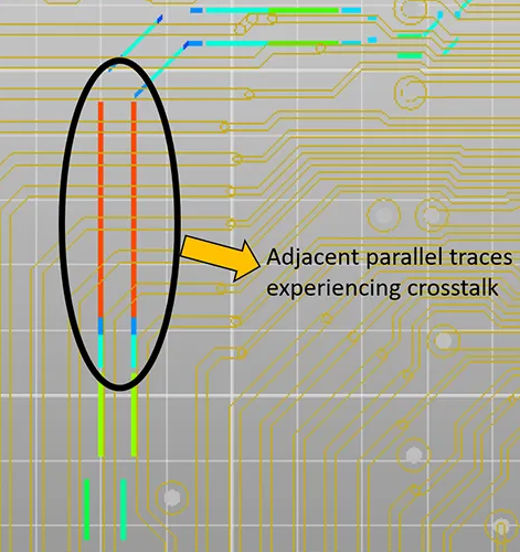
Understanding Crosstalk Mechanisms
Types of Crosstalk
Crosstalk manifests in two primary forms:
- Forward Crosstalk (Near-End Crosstalk – NEXT): Occurs at the end of the transmission line nearest to the signal source. The coupled noise appears in the same direction as the propagating aggressor signal.
- Backward Crosstalk (Far-End Crosstalk – FEXT): Appears at the far end of the victim line, opposite to the direction of the aggressor signal propagation.
Coupling Mechanisms
Crosstalk results from two fundamental coupling phenomena:
- Capacitive Coupling: Electric field interaction between conductors creates unwanted current flow
- Inductive Coupling: Magnetic field interaction induces voltage in nearby conductors
The relative significance of these mechanisms depends on factors like signal edge rates, trace geometry, and dielectric properties.
Key Factors Influencing Crosstalk
Several design parameters significantly affect crosstalk magnitude:
- Trace Spacing: The distance between adjacent traces directly impacts coupling strength
- Parallel Run Length: Longer parallel sections increase total coupled energy
- Reference Planes: The presence and quality of reference planes affect return paths
- Dielectric Material: The substrate’s dielectric constant influences electric field distribution
- Signal Edge Rates: Faster transitions generate stronger high-frequency components
- Trace Geometry: Width, thickness, and cross-sectional shape affect field distribution
PCB Routing Optimization Techniques
1. Strategic Trace Spacing
Implement the 3W rule (trace spacing ≥ 3× trace width) for critical signals. For high-density designs, use simulation to determine minimum acceptable spacing while maintaining signal integrity.
2. Minimize Parallel Run Length
Limit parallel routing of sensitive signals to essential sections only. When possible, route critical traces perpendicular to potential aggressors on adjacent layers.
3. Guard Traces and Shielding
Place grounded guard traces between sensitive signals to provide electrostatic shielding. For extremely sensitive circuits, consider full-coverage shielding with grounded copper.
4. Layer Stackup Optimization
Utilize stripline configurations (traces between reference planes) rather than microstrip (surface traces) for better containment of electromagnetic fields. Implement symmetrical layer stackups to balance coupling effects.
5. Differential Pair Routing
Maintain tight coupling within differential pairs while maximizing separation from other signals. Keep pair lengths matched to preserve common-mode rejection.
6. Impedance Control
Maintain consistent characteristic impedance throughout the signal path to minimize reflections that can exacerbate crosstalk effects.
7. Via Placement Optimization
Minimize via stubs and antipad sizes to reduce discontinuities. Place vias strategically to avoid creating coupling hotspots.
8. Signal Layer Assignment
Route high-speed signals on layers adjacent to solid reference planes. Separate sensitive analog and digital signals with ground planes when possible.
Advanced Techniques for High-Speed Designs
1. Orthogonal Routing on Adjacent Layers
Route traces perpendicular to each other on neighboring layers to minimize overlap and coupling.
2. Embedded Microstrip and Stripline
Utilize embedded trace configurations to contain electromagnetic fields more effectively than surface routing.
3. Grounded Coplanar Waveguides
Implement coplanar ground structures alongside critical traces to provide additional shielding.
4. Serpentine Routing for Length Matching
When length matching is required, use optimized serpentine patterns that minimize parallel sections.
5. Backdrilling for Via Stub Removal
In multilayer boards with high-frequency signals, employ backdrilling to remove unused via portions that can act as antennas.
Simulation and Verification Methods
1. 3D Electromagnetic Simulation
Use full-wave solvers to analyze complex coupling scenarios and validate design choices.
2. Time-Domain Reflectometry (TDR)
Measure actual impedance profiles to identify discontinuities that may contribute to crosstalk.
3. Eye Diagram Analysis
Evaluate signal quality metrics like jitter and noise margins under realistic operating conditions.
4. Near-Field Scanning
Identify electromagnetic hotspots and validate shielding effectiveness in physical prototypes.

Practical Implementation Considerations
1. Design Rule Development
Establish comprehensive design rules based on signal types, frequencies, and criticality.
2. Constraint Management
Implement constraint-driven design workflows to enforce spacing and routing requirements automatically.
3. Design Review Process
Incorporate crosstalk analysis as a formal step in the design review cycle.
4. Manufacturing Tolerances
Account for fabrication variations that may affect actual spacing and coupling in production boards.
Case Studies
1. High-Speed Memory Interface Optimization
Implementation of optimized routing reduced crosstalk-induced jitter by 42% in a DDR4 memory subsystem.
2. Mixed-Signal Board Improvement
Strategic layer assignment and guard traces improved SNR by 18dB in a high-precision data acquisition system.
3. RF Front-End Layout Enhancement
Careful impedance control and shielding techniques reduced unwanted coupling by 27dB in a multi-band radio design.
Future Trends and Challenges
As signal speeds continue to increase with technologies like PCIe 6.0 and DDR5, crosstalk management will require:
- More sophisticated 3D routing optimization tools
- Advanced materials with lower dielectric constants
- Integration of crosstalk prediction in real-time routing tools
- Machine learning approaches for automated routing optimization
Conclusion
Effective crosstalk reduction in PCB design requires a comprehensive approach combining fundamental understanding of coupling mechanisms with practical routing strategies. By implementing systematic spacing rules, optimizing layer stackups, employing shielding techniques, and leveraging advanced simulation tools, designers can significantly improve signal integrity in modern electronic systems. As technology advances, continuous refinement of these techniques will remain essential for maintaining reliable performance in increasingly dense and high-speed PCB designs.
The strategies presented in this paper provide a foundation for developing robust routing methodologies that balance performance requirements with practical manufacturing constraints. Design teams should adapt these principles to their specific applications while staying informed about emerging techniques in this critical aspect of PCB design.