PCB Design for Noise Suppression: Strategies and Techniques
Abstract
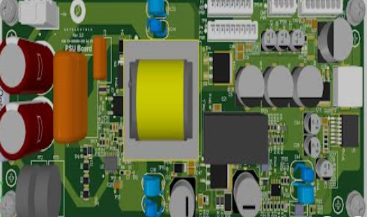
Printed Circuit Board (PCB) design plays a critical role in ensuring the reliability and performance of electronic systems. One of the key challenges in PCB design is managing electromagnetic interference (EMI), crosstalk, and other noise-related issues. This paper explores various techniques for suppressing noise in PCB designs, including proper grounding, shielding, trace routing, decoupling, and component placement. By implementing these strategies, designers can minimize interference, enhance signal integrity, and improve overall system performance.
1. Introduction
With the increasing complexity and miniaturization of electronic devices, PCB noise suppression has become a crucial aspect of circuit design. Noise can originate from multiple sources, including power supply fluctuations, high-speed signal switching, and external electromagnetic fields. If not properly managed, noise can lead to signal degradation, data corruption, and even system failure.
This paper discusses key PCB design techniques to mitigate noise, focusing on:
- Grounding strategies
- Power supply decoupling
- Signal integrity optimization
- Shielding and filtering techniques
- Component placement and routing best practices
2. Grounding Techniques for Noise Suppression
2.1 Single-Point vs. Multi-Point Grounding
Proper grounding is essential to minimize ground loops and noise coupling.
- Single-point grounding is effective in low-frequency applications where ground potential differences are minimal.
- Multi-point grounding is preferred for high-frequency circuits to reduce ground impedance and EMI.
2.2 Ground Plane Design
A solid ground plane helps in:
- Reducing ground impedance
- Providing a low-inductance return path for high-frequency signals
- Shielding sensitive traces from interference
Best Practices:
- Use a continuous ground plane without splits in high-speed designs.
- Avoid ground loops by ensuring proper return paths.
- Implement split ground planes for mixed-signal designs (analog and digital).
3. Power Supply Noise Reduction
3.1 Decoupling Capacitors
Decoupling capacitors suppress high-frequency noise in power distribution networks.
- Place bulk capacitors (10-100μF) near power inputs.
- Use small ceramic capacitors (0.1μF or smaller) near IC power pins.
3.2 Power Plane Design
- Use low-impedance power planes to minimize voltage drops.
- Implement power island techniques for sensitive circuits.
- Avoid overlapping high-speed signal traces with power planes..
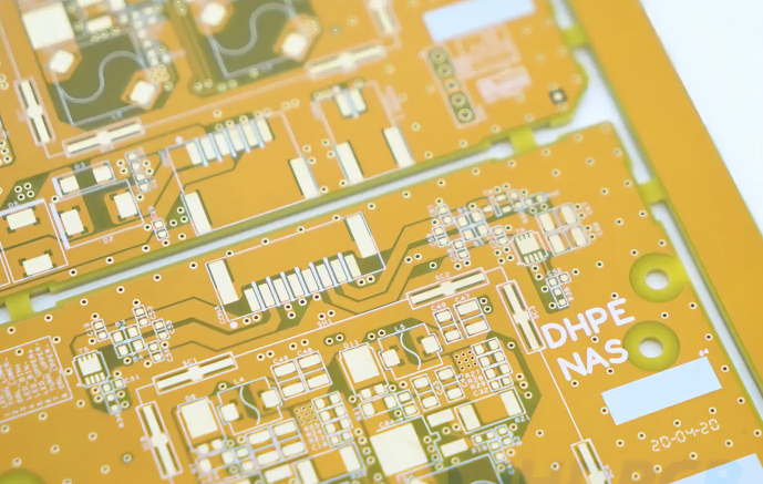
4. Signal Integrity and Trace Routing
4.1 Controlled Impedance Routing
- Match trace impedance to source and load to prevent reflections.
- Use microstrip or stripline configurations for high-speed signals.
4.2 Crosstalk Mitigation
- Maintain 3W rule (trace spacing ≥ 3× trace width) to reduce coupling.
- Route differential pairs closely to enhance noise immunity.
- Avoid parallel routing of high-speed and sensitive signals.
4.3 Minimizing Electromagnetic Radiation
- Use short and direct traces for high-frequency signals.
- Implement guard traces or ground vias near sensitive signals.
5. Shielding and Filtering
5.1 EMI Shielding
- Use metal enclosures or conductive coatings to block external interference.
- Implement grounded shields over sensitive components.
5.2 Filtering Techniques
- Ferrite beads suppress high-frequency noise on power lines.
- LC filters reduce conducted EMI.
- Common-mode chokes eliminate noise in differential signals.
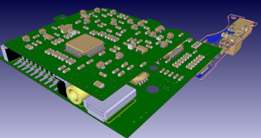
6. Component Placement Strategies
6.1 Partitioning and Zoning
- Separate analog, digital, and RF sections to prevent coupling.
- Place high-speed components away from sensitive analog circuits.
6.2 Thermal Management
- Proper heat dissipation reduces thermal noise.
- Use thermal vias and heatsinks for power components.
7. Advanced Noise Suppression Techniques
7.1 Embedded Capacitance
- Utilize power-ground plane capacitance for high-frequency decoupling.
7.2 Differential Signaling
- Reduces common-mode noise in high-speed interfaces (e.g., USB, HDMI).
7.3 Spread Spectrum Clocking
- Lowers peak EMI by modulating clock frequencies.
8. Conclusion
Effective PCB noise suppression requires a combination of proper grounding, power integrity management, signal routing optimization, and shielding techniques. By following these design principles, engineers can significantly reduce interference, enhance system reliability, and meet electromagnetic compatibility (EMC) standards. Future advancements in PCB materials and simulation tools will further improve noise suppression in high-speed and high-density designs.