The Usage of Pads and Vias in PCB Design
Introduction
Printed Circuit Board (PCB) design is a critical aspect of electronic product development. Among the various components and features in a PCB, pads and vias play essential roles in ensuring proper electrical connections, mechanical stability, and signal integrity. This article provides a comprehensive overview of the functions, types, and best practices for using pads and vias in PCB design.
1. Understanding Pads in PCB Design
1.1 Definition and Purpose
A pad is a conductive area on a PCB where components are soldered. Pads serve as the interface between component leads (or surface-mount device terminals) and the PCB’s copper traces.
1.2 Types of Pads
Pads can be categorized based on their mounting style and function:
1.2.1 Through-Hole Pads
- Used for components with leads that pass through holes in the PCB.
- Typically circular or oval-shaped.
- Provide strong mechanical bonding.
1.2.2 Surface-Mount (SMD) Pads
- Designed for surface-mount technology (SMT) components.
- Shapes include rectangular, rounded, and custom footprints.
- Smaller than through-hole pads, allowing higher component density.
1.2.3 BGA (Ball Grid Array) Pads
- Used for high-density IC packages.
- Small, circular pads arranged in a grid pattern.
- Require precise alignment and soldering techniques.
1.3 Pad Design Considerations
- Size & Shape: Must match component lead dimensions for proper soldering.
- Thermal Relief: Used in power planes to prevent excessive heat dissipation during soldering.
- Solder Mask & Paste Layers: Ensure proper solder application and prevent bridging.
2. Understanding Vias in PCB Design
2.1 Definition and Purpose
A via is a plated hole that connects different layers of a PCB, enabling electrical and thermal conduction between them.
2.2 Types of Vias
2.2.1 Through-Hole Vias
- Span the entire PCB thickness.
- Most common and cost-effective.
- Used for inter-layer connections and component mounting.
2.2.2 Blind Vias
- Connect an outer layer to an inner layer but do not go through the entire board.
- Used in high-density designs (e.g., HDI PCBs).
2.2.3 Buried Vias
- Connect inner layers without reaching outer layers.
- Improve routing density but increase manufacturing cost.
2.2.4 Microvias
- Small vias (typically < 150µm) used in HDI PCBs.
- Often laser-drilled for precision.
2.3 Via Design Considerations
- Size & Aspect Ratio: Smaller vias save space but must maintain manufacturability.
- Annular Ring: Ensures sufficient copper around the via hole for reliability.
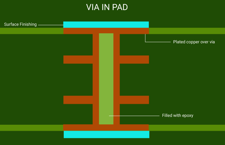
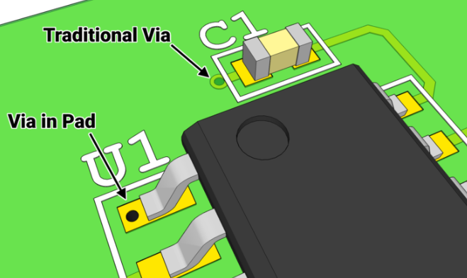
- Via-in-Pad: Used in high-speed designs but requires careful soldering.
- Tenting vs. Filling:
- Tenting: Covering vias with solder mask to prevent solder wicking.
- Filling: Filling vias with conductive/non-conductive material for planarization.
3. Best Practices for Using Pads and Vias
3.1 Pad Placement & Optimization
- Ensure adequate spacing between pads to prevent solder bridging.
- Use thermal relief pads for components requiring heat dissipation.
- Follow manufacturer guidelines for pad dimensions in SMD components.
3.2 Via Placement & Optimization
- Avoid placing vias under BGA pads unless necessary (via-in-pad requires filling).
- Use stitching vias in high-speed designs to reduce ground loops.
- Minimize via stubs in high-frequency PCBs to prevent signal reflections.
3.3 Manufacturing & Reliability Considerations
- Ensure proper via plating thickness to prevent cracking.
- Avoid excessive via drilling in flex PCBs to maintain flexibility.
- Use via shielding in RF designs to reduce interference.
4. Advanced Applications of Pads and Vias
4.1 High-Speed PCB Design
- Differential Pair Routing: Use vias carefully to maintain impedance matching.
- Via Shielding: Surround signal vias with grounded vias to reduce crosstalk.
4.2 High-Power PCB Design
- Thermal Vias: Improve heat dissipation in power components.
- Large Pads: Enhance current-carrying capacity in high-power circuits.
4.3 HDI (High-Density Interconnect) PCBs
- Microvias and stacked vias enable ultra-compact designs.
- Laser-drilled vias allow finer pitch routing.
5. Common Mistakes to Avoid
5.1 Pad-Related Errors
- Incorrect pad size leading to poor solder joints.
- Missing solder mask openings causing soldering issues.
5.2 Via-Related Errors
- Insufficient annular ring causing manufacturing defects.
- Excessive via stubs degrading signal integrity.
6. Conclusion
Pads and vias are fundamental elements in PCB design, influencing electrical performance, manufacturability, and reliability. Proper selection and optimization of these features are crucial for successful PCB layouts, especially in high-speed, high-power, and HDI applications. By following industry best practices and avoiding common pitfalls, designers can ensure robust and efficient PCB performance.