The Advantages and Disadvantagesof Blind and Buried Via PCB Stacked Via Design
Abstract
This paper explores the intricate aspects of blind and buried via stacked via design in printed circuit boards (PCBs), examining both the significant benefits and notable challenges associated with this advanced interconnection technology. As electronic devices continue to shrink in size while increasing in complexity and functionality, blind and buried vias—particularly in stacked configurations—have become essential tools for PCB designers. The article systematically analyzes the advantages including space savings, improved signal integrity, and enhanced design flexibility, while also addressing the drawbacks such as increased manufacturing complexity, higher costs, and potential reliability concerns. Through this balanced examination, the paper provides valuable insights for design engineers considering implementation of stacked blind and buried vias in high-density interconnect (HDI) PCB designs.
1. Introduction to Blind and Buried Vias
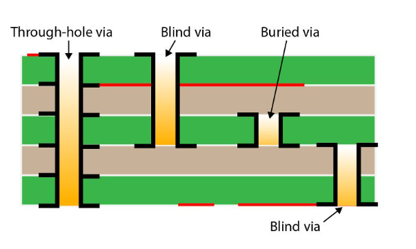
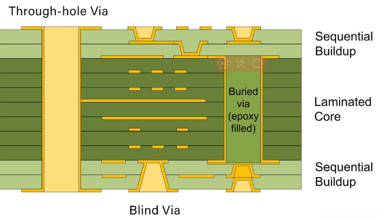
Blind and buried vias represent specialized types of interconnects in multilayer PCB designs that differ significantly from traditional through-hole vias. A blind via connects an outer layer of the board to one or more inner layers but does not pass completely through the entire board. A buried via, by contrast, connects inner layers without reaching either outer surface of the PCB. These via types enable more efficient use of board space and facilitate higher component density compared to conventional through-vias.
When these vias are stacked—aligned vertically through multiple layers—they create an even more compact interconnection system. Stacked via technology has become particularly valuable in modern HDI designs found in smartphones, tablets, wearable devices, and advanced computing systems where board real estate is at a premium.
2. Advantages of Stacked Blind and Buried Via Design
2.1 Space Optimization and Miniaturization
The most prominent advantage of stacked blind and buried vias is their unparalleled ability to conserve board space. In traditional through-hole via designs, each via occupies space on all layers of the board, significantly limiting routing channels. Stacked blind/buried vias:
- Occupy only the necessary layers
- Free up routing channels on unaffected layers
- Enable tighter component placement
- Facilitate overall board size reduction
This space efficiency allows for more compact product designs without sacrificing functionality, a critical factor in consumer electronics where every millimeter counts.
2.2 Enhanced Signal Integrity
Stacked via configurations can improve signal integrity in high-speed digital and high-frequency analog circuits by:
- Reducing via stub effects (especially with blind vias)
- Minimizing impedance discontinuities
- Shortening signal return paths
- Decreasing parasitic capacitance and inductance
Properly designed stacked vias maintain more consistent impedance characteristics compared to staggered via arrangements, reducing signal reflections and improving overall system performance.
2.3 Increased Design Flexibility
The implementation of stacked blind and buried vias provides PCB designers with greater layout flexibility:
- Enables escape routing from fine-pitch components (e.g., BGAs with <0.5mm pitch)
- Facilitates complex interconnect schemes in high-layer-count boards
- Allows more efficient power distribution network design
- Supports mixed-signal partitioning strategies
This flexibility becomes increasingly valuable as component densities continue to rise and product development cycles shorten.
2.4 Improved Thermal Management
Stacked vias can serve as effective thermal conduits in multilayer designs:
- Provide vertical heat dissipation paths
- Can be strategically placed under high-power components
- Allow for more even heat distribution across layers
- Enable connection to internal ground/power planes for heat spreading
This thermal management capability helps prevent localized hot spots that could affect reliability and performance.
3. Disadvantages and Challenges of Stacked Via Design
3.1 Manufacturing Complexity
Stacked blind and buried vias introduce significant fabrication challenges:
- Require precise layer-to-layer registration
- Need multiple lamination cycles for sequential buildup
- Demand strict process control for via filling and planarization
- Increase total board processing time
These factors make the manufacturing process more complex compared to conventional via structures, potentially affecting yield rates and requiring specialized equipment.
3.2 Higher Production Costs
The added manufacturing complexity directly translates to increased costs:
- Additional process steps (drilling, plating, lamination)
- Higher material costs (laser drills, fill materials)
- Greater need for quality control and testing
- Potential yield impacts from complex structures
For cost-sensitive applications, these factors may make stacked via designs economically unfeasible despite their technical benefits.
3.3 Reliability Concerns
Stacked via configurations introduce several reliability considerations:
- Increased risk of interfacial delamination due to multiple material interfaces
- Potential for via wall cracks from thermal cycling stresses
- Greater susceptibility to plating defects propagating through multiple layers
- Challenges in ensuring complete via filling and void elimination
These factors require careful design and process validation to ensure long-term reliability, particularly in harsh operating environments.
3.4 Design and Analysis Complexity
Implementing stacked vias effectively demands advanced design capabilities:
- Requires specialized CAD tools supporting 3D interconnect modeling
- Needs sophisticated signal integrity analysis for high-speed designs
- Demands careful consideration of manufacturing tolerances
- Benefits from design-for-manufacturing (DFM) expertise
This increased complexity may extend design cycles and require additional engineering resources.
4. Technical Considerations for Implementation
4.1 Material Selection
Choosing appropriate materials is crucial for successful stacked via implementation:
- Dielectric materials with compatible CTE (coefficient of thermal expansion)
- High-temperature stable substrates for multiple lamination cycles
- Compatible conductive fill materials
- Laser-drillable dielectrics for microvia formation
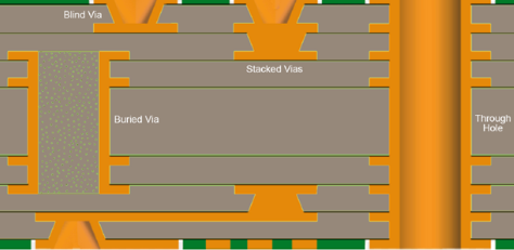
4.2 Stacking Configurations
Various stacking approaches offer different trade-offs:
- Fully stacked: Direct vertical alignment through multiple layers (maximum space savings)
- Staggered stacked: Offset alignment that reduces stress concentration
- Mixed stacking: Combination with other via types for optimal performance
4.3 Aspect Ratio Management
Maintaining appropriate aspect ratios (depth to diameter) is critical:
- Typical aspect ratios of 0.75:1 to 1:1 for reliable plating
- Consideration of via filling requirements
- Balance between current carrying capacity and manufacturability
5. Applications and Industry Trends
Stacked blind and buried via technology finds particular value in:
- Mobile devices: Smartphones, tablets requiring extreme miniaturization
- High-performance computing: Servers, network equipment with complex interconnects
- Automotive electronics: Space-constrained ADAS and infotainment systems
- Medical devices: Implantable and portable medical equipment
Industry trends show increasing adoption of stacked via designs, particularly with the growth of:
- 5G infrastructure requiring high-frequency performance
- AI hardware demanding dense interconnects
- IoT devices needing reliable compact packaging
6. Conclusion
Stacked blind and buried via designs offer PCB engineers powerful tools for meeting the challenges of modern electronics miniaturization and performance demands. The significant advantages in space savings, signal integrity, and design flexibility make these structures indispensable for many advanced applications. However, the associated manufacturing complexities, cost implications, and reliability considerations require careful evaluation on a case-by-case basis.
Successful implementation demands close collaboration between design and manufacturing teams, thorough understanding of material properties and process capabilities, and careful analysis of cost-performance trade-offs. As fabrication technologies continue to advance, many current limitations of stacked via designs are being addressed, promising even broader adoption in future electronic products.
For designers working on cutting-edge electronics, mastering stacked blind and buried via techniques has become an essential skill—one that balances the art of miniaturization with the science of reliable interconnection.