PCB Design Simulation: A Comprehensive Guide to Ensuring Optimal Performance
Introduction to PCB Design Simulation
Printed Circuit Board (PCB) design simulation has become an indispensable tool in modern electronics development, allowing engineers to verify and optimize their designs before physical prototyping. As electronic systems grow increasingly complex with higher speeds, greater component density, and more stringent performance requirements, simulation provides a cost-effective way to identify and resolve potential issues early in the design cycle.
PCB simulation encompasses various aspects of board performance, including signal integrity (SI), power integrity (PI), electromagnetic compatibility (EMC), thermal behavior, and mechanical stress. By leveraging advanced simulation tools, engineers can predict how their designs will behave in real-world conditions, reducing the number of design iterations and accelerating time-to-market.
This article explores the fundamental concepts, methodologies, and benefits of PCB design simulation, providing insights into current industry practices and emerging trends in this critical field of electronic design automation (EDA).
The Importance of Simulation in Modern PCB Design
Challenges in Contemporary PCB Design
Modern PCB designs face numerous challenges that make simulation essential:
- High-Speed Digital Circuits: With clock speeds exceeding several gigahertz and edge rates in the picosecond range, transmission line effects become significant, requiring careful analysis of signal propagation.
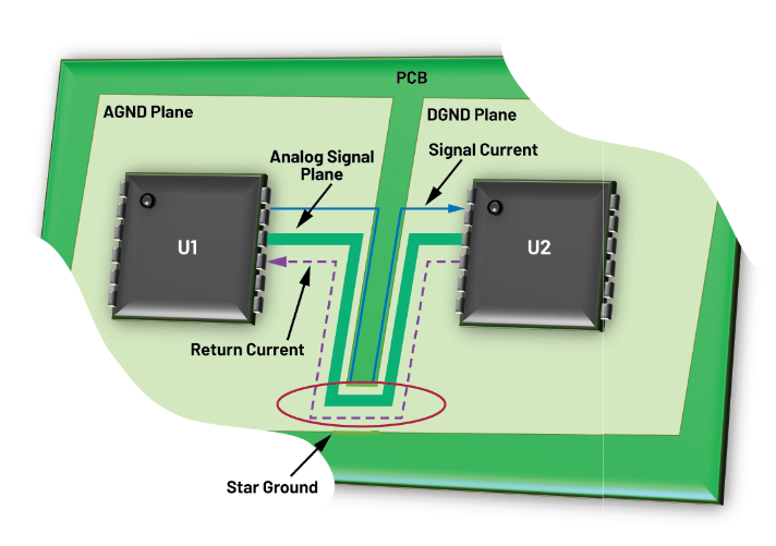
- Mixed-Signal Systems: The integration of analog and digital circuits on the same board creates complex interactions that must be managed to prevent performance degradation.
- Power Delivery Networks (PDNs): Modern processors and FPGAs demand high currents with tight voltage tolerances, making power distribution analysis crucial.
- EMC/EMI Considerations: Regulatory requirements and the need to prevent interference between system components necessitate thorough electromagnetic analysis.
- Thermal Management: Increasing power densities require careful thermal analysis to ensure reliable operation.
Benefits of Simulation
PCB design simulation offers numerous advantages:
- Cost Reduction: Identifying and fixing problems during design is far less expensive than after manufacturing.
- Time Savings: Simulation accelerates the design cycle by reducing prototype iterations.
- Performance Optimization: Engineers can explore design alternatives to achieve optimal performance.
- Risk Mitigation: Potential reliability issues can be identified and addressed before production.
- Virtual Prototyping: Enables testing of designs under various conditions that may be difficult or expensive to recreate physically.
Key Areas of PCB Design Simulation
Signal Integrity (SI) Analysis
Signal integrity simulation focuses on ensuring clean, undistorted signal transmission across PCB interconnects. Key aspects include:
- Transmission Line Analysis: Modeling traces as transmission lines to analyze impedance matching, reflections, and signal quality.
- Crosstalk Analysis: Quantifying unwanted coupling between adjacent signals.
- Timing Analysis: Verifying signal propagation delays meet timing budgets.
- Eye Diagram Analysis: Assessing signal quality in high-speed serial links.
Modern SI tools use sophisticated algorithms to model these effects, often incorporating S-parameter models for high-frequency behavior.
Power Integrity (PI) Analysis
Power integrity simulation ensures stable power delivery to all components:
- DC Analysis: Verifying voltage drops across the power distribution network.
- AC Analysis: Assessing impedance of the PDN across frequency.
- Decoupling Optimization: Determining optimal capacitor selection and placement.
- Simultaneous Switching Noise (SSN): Analyzing noise generated when multiple outputs switch simultaneously.
PI tools typically combine circuit simulation with electromagnetic field solvers for accurate results.
Electromagnetic Compatibility (EMC) Simulation
EMC simulation helps predict and mitigate electromagnetic interference:
- Radiated Emissions: Predicting unwanted radiation from the board.
- Radiated Susceptibility: Assessing vulnerability to external fields.
- Conducted Emissions: Analyzing noise propagating through power and ground.
- Shielding Effectiveness: Evaluating enclosure performance.
Full-wave 3D electromagnetic solvers are often employed for comprehensive EMC analysis.

Thermal Analysis
Thermal simulation predicts temperature distribution and heat flow:
- Component Junction Temperatures: Ensuring devices operate within specifications.
- Heat Spreader Effectiveness: Evaluating thermal vias, planes, and heatsinks.
- Airflow Analysis: Modeling convection cooling in enclosures.
- Thermal Stress: Identifying potential reliability issues from thermal cycling.
Computational fluid dynamics (CFD) tools are commonly used for detailed thermal analysis.
Mechanical Simulation
Mechanical aspects of PCB design may also require simulation:
- Vibration Analysis: Assessing board response to mechanical vibration.
- Stress Analysis: Predicting mechanical stresses during assembly and operation.
- Warpage Prediction: Analyzing potential board deformation during manufacturing.
Finite element analysis (FEA) tools are typically employed for these simulations.
Simulation Methodologies and Tools
Simulation Workflow
A typical PCB simulation workflow includes:
- Pre-Layout Analysis: Early-stage exploration of design constraints and requirements.
- In-Design Verification: Continuous checking during layout to catch issues early.
- Post-Layout Verification: Comprehensive analysis of the completed design.
- Correlation Studies: Comparing simulation results with physical measurements to validate models.
Types of Simulation Tools
- Circuit Simulators: SPICE-based tools for analog and mixed-signal simulation.
- 2.5D Field Solvers: For analysis of planar structures like PCBs.
- 3D Full-Wave Solvers: For detailed electromagnetic analysis of complex structures.
- Thermal Simulators: For temperature and airflow prediction.
- Multi-Physics Tools: Combining multiple simulation domains.
Popular PCB Simulation Software
- ANSYS Electronics Desktop: Comprehensive suite for SI, PI, and thermal analysis.
- Cadence Sigrity: Specialized for power and signal integrity.
- Keysight ADS: Advanced high-frequency and high-speed digital simulation.
- Altium Designer: Integrated PCB design with basic simulation capabilities.
- Mentor HyperLynx: Focused on signal and power integrity.
- COMSOL Multiphysics: For complex multi-physics simulations.
Best Practices in PCB Design Simulation
Model Accuracy
- Component Models: Use accurate models for all critical components (IBIS, SPICE, S-parameters).
- Material Properties: Specify correct dielectric constants, loss tangents, and copper roughness.
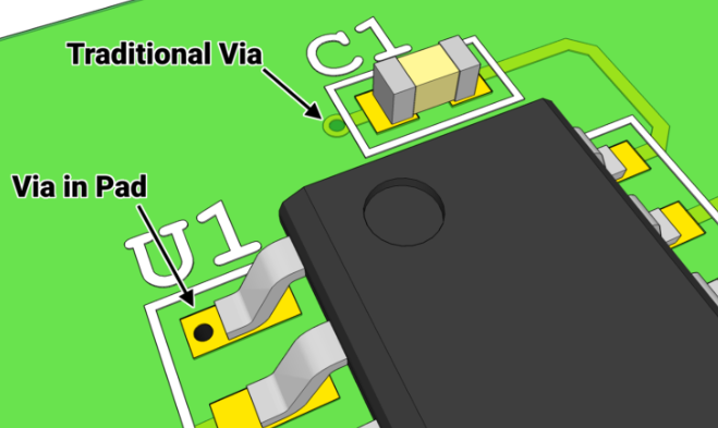
- Interconnect Modeling: Account for via effects, trace roughness, and 3D geometry where significant.
Simulation Setup
- Mesh Refinement: Ensure adequate mesh resolution without excessive computation time.
- Frequency Range: Select appropriate frequency ranges for the analysis.
- Port Definitions: Properly define excitation and measurement ports.
- Convergence Criteria: Set appropriate tolerances for solution convergence.
Interpretation of Results
- Understand Limitations: Recognize the approximations and assumptions in each simulation.
- Critical Metrics: Focus on key performance indicators relevant to the design goals.
- Sensitivity Analysis: Identify which parameters have the greatest impact on performance.
- Design Margins: Incorporate appropriate safety margins to account for manufacturing variations.
Advanced Simulation Techniques
Statistical Analysis and Variation Modeling
- Monte Carlo Analysis: Assessing the impact of parameter variations.
- Process Variation Modeling: Accounting for manufacturing tolerances.
- Corner Analysis: Evaluating performance at extreme parameter values.
Co-Simulation Approaches
- SI/PI Co-Simulation: Combined analysis of signal and power integrity interactions.
- Thermal-Electrical Co-Simulation: Modeling the interplay between temperature and electrical performance.
- EMC-System Co-Simulation: Integrating board-level EMC with system-level analysis.
Machine Learning in PCB Simulation
Emerging techniques include:
- Surrogate Modeling: Using ML to create fast approximate models of complex simulations.
- Automated Optimization: ML-driven design optimization.
- Anomaly Detection: Identifying potential issues in simulation results.
Future Trends in PCB Design Simulation
- Increased Integration: Tighter coupling between design and simulation tools.
- Cloud-Based Simulation: Leveraging cloud computing for complex analyses.
- AI-Assisted Simulation: Intelligent automation of setup and analysis.
- Multi-Physics Integration: More comprehensive coupled simulations.
- Virtual Reality Visualization: Immersive exploration of simulation results.
Conclusion
PCB design simulation has evolved into a sophisticated discipline that is critical for developing reliable, high-performance electronic systems. By enabling virtual prototyping and performance verification, simulation tools significantly reduce development costs and time-to-market while improving product quality.
As electronic systems continue to increase in complexity, the role of simulation will only grow more important. Engineers who master these tools and methodologies will be well-positioned to tackle the challenges of next-generation PCB design, from high-speed digital systems to RF and mixed-signal applications.
The future of PCB simulation lies in greater integration, automation, and multi-physics capabilities, promising even more powerful tools for electronic design innovation. By embracing these advanced simulation techniques, design teams can push the boundaries of performance while maintaining reliability and manufacturability in an increasingly competitive marketplace.