Planning and Handling of Ground and Power Lines in PCB Routing
1. Introduction
Printed Circuit Board (PCB) design is a critical aspect of electronic product development, where proper routing of power and ground lines significantly impacts performance, signal integrity, and electromagnetic compatibility (EMC). Poorly designed power and ground networks can lead to noise coupling, voltage drops, and even circuit malfunction. This article explores best practices for planning and handling ground and power lines in PCB routing, covering key concepts such as grounding strategies, power distribution networks (PDNs), and noise reduction techniques.
2. Importance of Proper Ground and Power Routing
2.1 Signal Integrity and Noise Reduction
- Ground loops and improper power distribution can introduce noise, leading to signal degradation.
- High-speed digital circuits and analog systems are particularly sensitive to power supply fluctuations and ground bounce.
2.2 Electromagnetic Compatibility (EMC)
- Poor grounding can result in electromagnetic interference (EMI), affecting both the PCB and nearby electronic devices.
- A well-designed ground plane minimizes radiated emissions and susceptibility to external noise.
2.3 Thermal Management
- Power traces carry high currents, and improper routing can lead to excessive heat buildup, affecting component reliability.
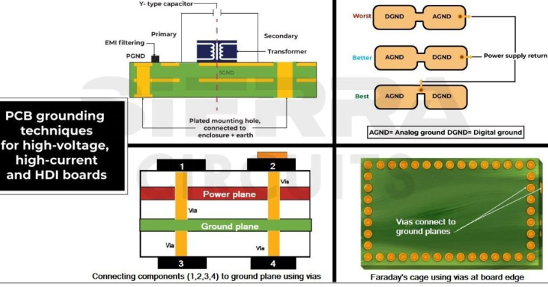
3. Grounding Strategies in PCB Design
3.1 Single-Point vs. Multi-Point Grounding
- Single-Point Grounding: Used in low-frequency circuits to avoid ground loops. All ground connections meet at a single node.
- Multi-Point Grounding: Preferred for high-frequency designs, where ground connections are distributed across the PCB to minimize inductance.
3.2 Ground Planes
- A solid ground plane provides a low-impedance return path for signals and reduces EMI.
- Split ground planes may be used to isolate analog and digital grounds, but they must be connected at a single point to prevent voltage differences.
3.3 Star Grounding
- Critical in mixed-signal designs, where sensitive analog and digital grounds are connected at a central point to minimize interference.
4. Power Distribution Network (PDN) Design
4.1 Power Plane vs. Power Traces
- Power planes offer low impedance and better current distribution, ideal for high-speed and high-current applications.
- Power traces are used when a full plane isn’t feasible, but they must be sufficiently wide to handle current without excessive voltage drop.
4.2 Decoupling Capacitors
- Placed near IC power pins to suppress high-frequency noise and stabilize voltage.
- Use a combination of bulk capacitors (for low-frequency stability) and ceramic capacitors (for high-frequency decoupling).
4.3 Power Supply Filtering
- Ferrite beads and LC filters help reduce high-frequency noise in power lines.
- Proper placement of voltage regulators ensures clean power delivery.
5. PCB Layer Stackup Considerations
5.1 Multilayer PCB Design
- A 4-layer PCB typically follows: Signal – Ground – Power – Signal.
- High-speed designs may use additional ground layers to minimize crosstalk.
5.2 Controlled Impedance Routing
- Critical for high-speed signals; ground planes provide reference for impedance matching.
- Avoid splitting ground planes under high-speed traces to prevent impedance discontinuities.

6. Handling High-Current Traces
6.1 Trace Width Calculation
- Use PCB trace width calculators to determine appropriate widths based on current load (e.g., IPC-2152 standards).
- Wider traces reduce resistance and heat dissipation.
6.2 Via Placement for Power Lines
- Multiple vias distribute current and reduce inductance in high-current paths.
- Avoid daisy-chaining power connections; instead, use a star topology.
7. Noise Reduction Techniques
7.1 Minimizing Ground Loops
- Ensure ground return paths are as short as possible.
- Avoid routing sensitive signals across split ground planes.
7.2 Shielding and Guard Traces
- Guard traces with grounded vias can isolate sensitive signals from noise sources.
- Use ground-filled areas around high-frequency components.
7.3 Differential Pair Routing
- For high-speed signals (e.g., USB, HDMI), route differential pairs with tight coupling and equal-length traces to minimize EMI.
8. Common Mistakes in Ground and Power Routing
8.1 Floating Ground Islands
- Unconnected ground sections can act as antennas, radiating noise.
- Always ensure all ground regions are properly connected.
8.2 Insufficient Decoupling
- Missing or improperly placed decoupling capacitors lead to power supply instability.
- Follow manufacturer recommendations for capacitor placement.
8.3 Overlooking Return Current Paths
- High-speed signals follow the path of least inductance, which is directly under the trace on the ground plane.
- Disruptions in the ground plane can cause signal integrity issues.
9. Advanced Techniques
9.1 Power Integrity Simulation
- Tools like SI/PI (Signal Integrity/Power Integrity) analysis help optimize PDN performance.
- Identify voltage drop and resonance issues before fabrication.
9.2 Embedded Passives
- Integrating decoupling capacitors within the PCB layers saves space and improves high-frequency performance.
9.3 Hybrid Grounding for Mixed-Signal PCBs
- Combines single-point and multi-point grounding to optimize both analog and digital performance.
10. Conclusion
Effective planning and handling of ground and power lines in PCB routing are essential for ensuring signal integrity, reducing noise, and maintaining EMC compliance. By implementing proper grounding strategies, optimizing power distribution networks, and following best practices in trace routing, designers can enhance PCB reliability and performance. Advanced techniques such as power integrity simulations and hybrid grounding further refine the design process, making it crucial for engineers to stay updated with evolving PCB design methodologies.